
Q.No:1 JAM-2015
Temperature dependence of resistivity of a metal can be described by
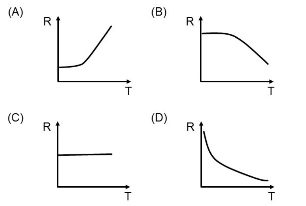
Check Answer
Option A
Q.No:2 JAM-2015
Consider a 20\(\mu\)m diameter p-n junction fabricated in silicon. The donor density is \(10^{16}\) per \(cm^3\). The charge developed on the n-side is \(1.6\times 10^{-13}\)C. Then the width (in \(\mu\)m) of the depletion region on the n-side of the p-n junction is _____________.
Check Answer
Ans 0.30-0.35
Q.No:3 JAM-2016
A \(pn\) junction was formed with a heavily doped \((10^{18}cm^{-3}\) \(p\)-region and lightly doped \((10^{14}cm^{-3}\) \(n\)-region. Which of the following statement(s) is(are) correct?
(A)
The width of the depletion layer will be more in the \(n\)-side of the junction.
(B)
The width of the depletion layer will be more in the \(p\)-side of the junction.
(C)
The width of the depletion layer will be same on both sides of the junction.
(D)
If the \(pn\) junction is reverse biased, then the width of the depletion region increases.
Check Answer
Option A,D
Q.No:4 JAM-2017
Which one of the following schematic curves best represents the variation of conductivity \(\sigma\) of a metal with temperature \(T\) ?

Check Answer
Option B
Q.No:5 JAM-2017
An intrinsic semiconductor of band gap \(1.25\)eV has an electron concentration \(10^{10}\)\(cm^{-3}\) at 300K. Assume that its band gap is independent of temperature and that the electron
concentration depends only exponentially on the temperature. If the electron concentration at 200K is \(Y\times 10^N \hspace{1mm} cm^{-3}(1<Y<10; N\)=Integer), then the value of \(N\) is ____________________.
Check Answer
Ans 4
Q.No:6 JAM-2018
In a pn junction, dopant concentration on the p-side is higher than that on the n-side. Which of the following statements is (are) correct, when the junction is unbiased?
(A)
The width of the depletion layer is larger on the n-side.
(B)
At thermal equilibrium the Fermi energy is higher on the p-side
(C)
In the depletion region, number of negative charges per unit area on the p-side is equal to number of positive charges per unit area on the n-side.
(D)
The value of the built-in potential barrier depends on the dopant concentration.
Check Answer
Option A,C,D
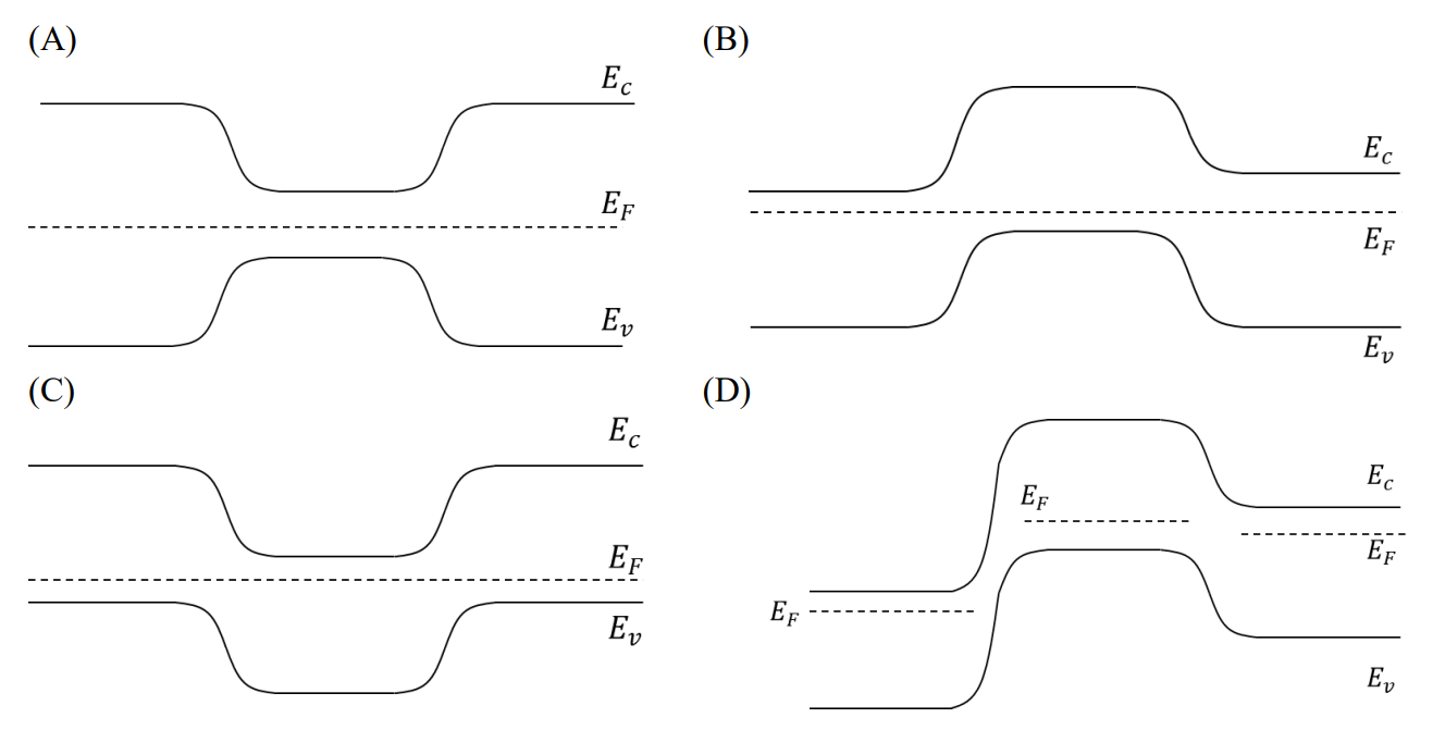
Q.No:7 JAM-2019
For a forward biased p-n junction diode, which one of the following energy-band diagrams is correct?
(\(\epsilon_F\) is the Fermi energy)

Check Answer
Option A
Q.No:8 JAM-2020
For an unbiased Silicon n-p-n transistor in thermal equilibrium, which one of the following electronic energy band diagrams is correct? (\(E_c\) =conduction band minimum, \(E_v\)= valence band maximum, \(E_F\)= Fermi level).
Check Answer
Option B
Q.No:9 JAM-2021
For a semiconductor material, the conventional flat band energy diagram is shown in the figure. The variables Y, X, respectively, are
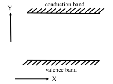
(A)
Energy, Momentum
(B)
Energy, Distance
(C)
Distance, Energy
(D)
Momentum, Energy
Check Answer
Option B
Q.No:10 JAM-2021
A semiconductor pn junction at thermal equilibrium has the space charge density \(\rho(x)\) profile as shown in the figure. The figure that best depicts the variation of the electric field \(E\) with \(x\) is (\(W\) denotes the width of the depletion layer)


Check Answer
Option A
Q.No:11 JAM-2022
For an ideal intrinsic semiconductor, the Fermi energy at 0\(K\)
(A)
lies at the top of the valence band
(B)
lies at the bottom of the conduction band
(C)
lies at the center of the bandgap
(D)
lies midway between center of the bandgap and bottom of the conduction band
Check Answer
Option C
Q.No:12 JAM-2022
For an n-type silicon, an extrinsic semiconductor, the natural logarithm of normalized conductivity \((\sigma)\) is plotted as a function of inverse temperature. Temperature interval-I corresponds to the intrinsic regime, interval-II corresponds to saturation regime and interval-III corresponds to the freeze-out regime, respectively. Then

(A)
the magnitude of the slope of the curve in the temperature interval-I is proportional to the bandgap, \(E_g\)
(B)
the magnitude of the slope of the curve in the temperature interval-III is proportional to the ionization energy of the donor, \(E_d\)
(C)
in the temperature interval-II, the carrier density in the conduction band is equal to the density of donors
(D)
in the temperature interval-III, all the donor levels are ionized
Check Answer
Option A,B,C
Q.No:13 JAM-2022
Consider a p-n junction at T = 300 K. The saturation current density at reverse bias is −20 \(\mu A/cm^2\). For this device, a current density of magnitude 10 \(\mu A/cm^2\) is realized with a forward bias voltage, \(V_F\) The same magnitude of current density can also be realized with a reverse bias voltage, \(V_R\). The value of \(|V_F/V_R|\) is ________________ (Round off to 2 decimal places).
Check Answer
Ans 0.57-0.61
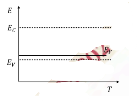
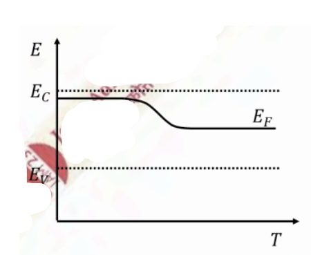
Q.No:14 JAM-2023
In an extrinsic p-type semiconductor, which of the following schematic diagram depicts the variation of the Fermi energy level (\(E_F\)) with temperature (\(T\))?
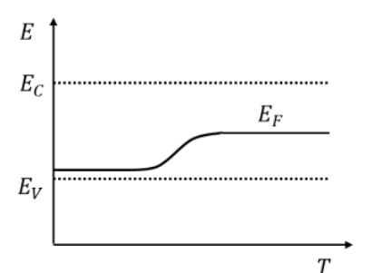

Check Answer
Option A
Q.No:15 JAM-2024
Consider a \( p\)-\( n \) junction diode which has \( 10^{23} \) acceptor-atoms/\( m^3 \) in the \( p \)-side and \( 10^{22} \) donor-atoms/\( m^3 \) in the \( n \)-side. If the depletion width in the \( p \)-side is \( 0.16 \mu m \), then the value of depletion width in the \( n \)-side will be_________________\( \mu m \). (Rounded off to one decimal place)
Check Answer
Ans 1.6
Q.No:16 JAM-2024
A pure Si crystal can be converted to an \( n \)-type crystal by doping with:
A) P
B) As
C) Sb
D) In