
Q.No:1 CSIR Dec-2014
The least significant bit of an 8-bit binary number is zero. A binary number whose value is \(8\) times the previous number has
(1)
\(12\) bits ending with three zeros
(2)
\(11\) bits ending with four zeros
(3)
\(11\) bits ending with three zeros
(4)
\(12\) bits ending with four zeros
Check Answer
Option 2
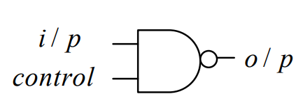
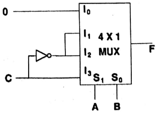
Q.No:2 CSIR June-2015
Which of the following circuits behaves as a controlled inverter?


Check Answer
Option 2_4
Q.No:2 CSIR June-2015
For the logic circuit given below, the decimal count sequence and the modulus of the circuit corresponding to A B C D are

(1)
\(8\rightarrow4\rightarrow2\rightarrow1\rightarrow9\rightarrow5(mod 6)\)
(2)
\(8\rightarrow4\rightarrow2\rightarrow9\rightarrow5\rightarrow3(mod 6)\)
(3)
\(2\rightarrow5\rightarrow9\rightarrow1\rightarrow3(mod 5)\)
(4)
\(8\rightarrow5\rightarrow1\rightarrow3\rightarrow7(mod 5)\)
Check Answer
Option 2
Q.No:4 CSIR Dec-2015
In the schematic figure given below, the initial values of \(4\) bit shift registers A and B are 1011 and 0010 respectively. The values at \(\text{SO}_{\text{A}}\) and \(\text{SO}_{\text{B}}\) after the pulse \(T_2\) are respectively

(1)
1110 and 1001
(2)
1101 and 1001
(3)
1101 and 1100
(4)
1110 and 1100
Check Answer
Option 4
Q.No:5 CSIR Dec-2015
The state diagram corresponding to the following circuit is


Check Answer
Option 4
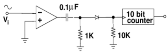
Q.No:6 CSIR Dec-2015
A sinusoidal signal of peak to peak amplitude \(1 \text{ V}\) and unknown time period is input to the following circuit for \(5\) seconds duration. If the counter measures a value \((3\text{E}8)_{\text{H}}\) in hexadecimal then the time period of the input signal is
(1)
\(2.5 \text{ ms}\)
(2)
\(10 \text{ ms}\)
(3)
\(4 \text{ ms}\)
(4)
\(5 \text{ ms}\)
Check Answer
Option 4
Q.No:7 CSIR June-2016
In the schematic figure given below, assume that the propagation delay of each logic gate is \(t_{\text{gate}}\).

The propagation delay of the circuit will be maximum when the logic inputs A and B make the transition
(1)
\((0, 1)\to (1, 1)\)
(2)
\((1, 1)\to (0, 1)\)
(3)
\((0, 0)\to (1, 1)\)
(4)
\((0, 0)\to (0, 1)\)
Check Answer
Option 4
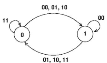
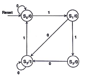
Q.No:8 CSIR June-2016
The state diagram that detects three or more consecutive 1's in a serial bit stream is


Check Answer
Option 4
Q.No:9 CSIR Dec-2016
Which of the following circuits implements the Boolean function \(F(A, B, C)=\sum (1, 2, 4, 6)\)?


Check Answer
Option 2
Q.No:10 CSIR June-2017
A \(2\times 4\) decoder with an enable input can function as a
(1)
\(4\times 1\) multiplexer
(2)
\(1\times 4\) demultiplexer
(3)
\(4\times 2\) encoder
(4)
\(4\times 2\) priority encoder
Check Answer
Option 2
Q.No:11 CSIR June-2017
In the figures below, X and Y are one bit inputs. The circuit which corresponds to a one bit comparator is


Check Answer
Option 3
Q.No:12 CSIR Dec-2017
The full scale voltage of an \(n\)-bit Digital-to-Analog Converter is \(V\). The resolution that can be achieved in it is
(1)
\(V/(2^n-1)\)
(2)
\(V/(2^n+1)\)
(3)
\(V/2^{2n}\)
(4)
\(V/n\)
Check Answer
Option 1
Q.No:13 CSIR Dec-2017
The circuit below comprises of D-flip flops. The output is taken from \(Q_3, Q_2, Q_1\) and \(Q_0\), as shown in the figure.

The binary number given by the string \(Q_3 Q_2 Q_1 Q_0\) changes for every clock pulse that is applied to the CLK input. If the output is initialized at 0000, then the corresponding sequence of decimal numbers that repeats itself, is
(1)
3, 2, 1, 0
(2)
1, 3, 7, 14, 12, 8
(3)
1, 3, 7, 15, 12, 14, 0
(4)
1, 3, 7, 15, 14, 12, 8, 0
Check Answer
Option 4
Q.No:14 CSIR June-2018
Which of the following gates can be used as a parity checker?
(1)
an OR gate
(2)
a NOR gate
(3)
an exclusive OR (XOR) gate
(4)
an AND gate
Check Answer
Option 3
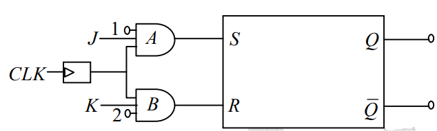
Q.No:15 CSIR June-2018
In the following JK flip-flop circuit, J and K inputs are tied together to \(+V_{CC}\). If the input is a clock signal of frequency \(f\), the frequency of the output Q is

(1)
\(f\)
(2)
\(2f\)
(3)
\(4f\)
(4)
\(f/2\)
Check Answer
Option 4
Q.No:16 CSIR June-2018
The full scale of a 3-bit digital-to-analog (DAC) converter is \(7 V\). Which of the following tables represents the output voltage of this 3-bit DAC for the given set of input bits?

Check Answer
Option 1
Q.No:17 CSIR Dec-2018
Consider the following circuit, consisting of an RS flip-flop and two AND gates.
Which of the following connections will allow the entire circuit to act as a JK flip-flop?
(1)
connect \(Q\) to pin 1 and \(\overline{Q}\) to pin 2
(2)
connect \(Q\) to pin 2 and \(\overline{Q}\) to pin 1
(3)
connect \(Q\) to \(K\) input and \(\overline{Q}\) to \(J\) input
(4)
connect \(Q\) to \(J\) input and \(\overline{Q}\) to \(K\) input
Check Answer
Option 2
Q.No:18 CSIR Dec-2018
The truth table below gives the value \(Y(A, B, C)\) where \(A, B\) and \(C\) are binary variables.

The output \(Y\) can be represented by
(1)
\(Y=\bar{A}\bar{B}C+\bar{A}B\bar{C}+A\bar{B}C+AB\bar{C}\)
(2)
\(Y=\bar{A}\bar{B}\bar{C}+\bar{A}BC+A\bar{B}\bar{C}+ABC\)
(3)
\(Y=\bar{A}\bar{B}C+\bar{A}BC+A\bar{B}C+ABC\)
(4)
\(Y=\bar{A}\bar{B}\bar{C}+\bar{A}B\bar{C}+A\bar{B}\bar{C}+AB\bar{C}\)
Check Answer
Option 2
Q.No:19 CSIR June-2019
Let \(Y\) denote the output in the following logical circuit.

If \(Y=AB+\bar{C}\bar{D}\), the gates \(G_1\) and \(G_2\) must, respectively, be
(1)
OR and NAND
(2)
NOR and OR
(3)
AND and NAND
(4)
NAND and OR
Check Answer
Option 2
Q.No:20 CSIR Dec-2019
The figure below shows a \(2\)-bit simultaneous analog-to-digital (A/D) converter operating in the voltage range \(0\) to \(V_0\). The output of the comparators are \(C_1, C_2\) and \(C_3\) with the reference inputs \(V_0/4, V_0/2\) and \(3V_0/4\), respectively.

The logic expression for the output corresponding to the less significant bit is
(1)
\(C_1 C_2 C_3\)
(2)
\(C_2 \bar{C}_3+\bar{C}_1\)
(3)
\(C_1 \bar{C}_2+C_3\)
(4)
\(C_2 \bar{C}_3+C_2\)
Check Answer
Option 3
Q.No:21 Assam CSIR Dec-2019
A combinational digital logic circuit has three inputs and one output. When the decimal equivalent of the binary inputs A (most significant bit), B and C (least significant bit) is less than \(3\), the circuit produces the output as LOW. The simplified logic expression for the output is
(1)
\(A+(B\cdot C)\)
(2)
\(\overline{A\cdot B\cdot C}\)
(3)
\(A\cdot B\cdot C\)
(4)
\(\overline{(\overline{A\cdot B})\cdot \overline{C}}\)
Check Answer
Option 1
Q.No:22 Assam CSIR Dec-2019
Temperature in the range of \(-10^{\circ}C\) to \(50^{\circ}C\) is to be measured with an analog to digital converter (ADC) with a resolution of \(0.01^{\circ}C\). The minimum number of bits required for the ADC to meet this requirement is
(1)
\(12\)
(2)
\(9\)
(3)
\(14\)
(4)
\(13\)
Check Answer
Option 4
Q.No:23 Assam CSIR Dec-2019
In the digital circuit shown below, the inputs are \(X_0\) and \(X_1\), and the delay \(\Delta\) in the paths are in time scale of \({ns}\) (nanosecond).
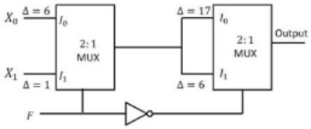
The propagation delay of the inverter is \(1 ns\) and that of each of the \(2:1\) multiplexers (MUX) obeying the truth table \(\begin{bmatrix}F&\text{Output}\\0&I_0\\1&I_1\end{bmatrix}\), is \(3 ns\). The time delay between the input and the output of the circuit when the select signal \(F=0\), is
(1)
\(18 ns\)
(2)
\(13 ns\)
(3)
\(24 ns\)
(4)
\(19 ns\)
Check Answer
Option 1
Q.No:24 Assam CSIR Dec-2019
Assume all the three J-K flip-flops in the digital circuit shown below are initialised with \(A=B=C=0\).
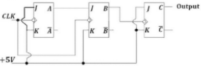
If the frequency of the clock signal (\(CLK\)) is \(96 kHz\) with \(50\%\) duty cycle, then the frequency of the output signal is
(1)
\(96 kHz\)
(2)
\(48 kHz\)
(3)
\(32 kHz\)
(4)
\(24 kHz\)
Check Answer
Option 4
Q.No:25 CSIR June-2020
In the 3-bit register shown below, \(Q_1\) and \(Q_3\) are the least and the most significant bits of the output, respectively.

If \(Q_1, Q_2\) and \(Q_3\) are set to zero initially, then the output after the arrival of the second falling clock (CLK) edge is
(a)
001
(b)
100
(c)
011
(d)
110
Check Answer
Option c
Q.No:26 CSIR June-2020
The Boolean equation \(Y=\bar{A}BC+\bar{A}B\bar{C}+A\bar{B}\bar{C}+A\bar{B}C\) is to be implemented using only two-input NAND gates. The minimum number of gates required is
(a)
\(3\)
(b)
\(4\)
(c)
\(5\)
(d)
\(6\)
Check Answer
Option b
Q.No:27 CSIR Feb-2022
The door of an X -ray machine room is fitted with a sensor D ( 0 is open and 1 is closed).
It is also equipped with three fire sensors \(F_1 , F_2\) and \(F_3\) (each is 0 when disabled and 1 when
enabled). The X -ray machine can operate only if the door is closed and at least 2 fire sensors
are enabled. The logic circuit to ensure that the machine can be operated is
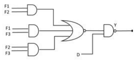


Check Answer
Option 2
Q.No:28 CSIR Sep-2022
A liquid oxygen cylinder system is fitted with a level-censor \((L)\) and a pressure-censor \((P)\), as shown in the figure below. The outputs of \(L\) and \(P\) are set to logic high \((S=1)\) when the measured value exceed the respective preset threshold values. The system can be shut off either by an operator by setting the input \(S\) to high, or when the level of oxygen in the tanks falls below the threshold value
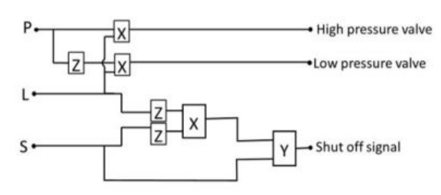
The logic gates X, Y and Z, respectively, are
(1)
OR, AND and NOT
(2)
AND, OR and NOT
(3)
NAND, OR and NOT
(4)
NOR, AND and NOT
Check Answer
Option 2
Q.No:28 CSIR June-2023
A train of impulses of frequency \(500 \hspace{1mm}Hz\), in which the temporal width of each spike is negligible compared to its period, is used to sample a sinusoidal input signal of frequency \(100 \hspace{1mm}Hz\). The sampled output is
1) discrete with the spacing between the peaks being the same as the time period of the sampling signal
2) a sinusoidal wave with the same time period as the sampling signal
3) discrete with the spacing between the peaks being the same as the time period of the input signal
4) a sinusoidal wave with the same time period as the input signal
Check Answer
Option 1
Q.No:29 CSIR June-2023
For the given logic circuit, the input waveforms A, B, C and D are shown as a function of time.
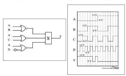
To obtain the output Y as shown in the figure, the logic gate X should be
1) an AND gate
2) an OR gate
3) a NAND gate
4) a NOR gate
Check Answer
Option 2
Q.No:30 CSIR Dec-2023
For three inputs \( A \), \( B \) and \( C \), the minimum number of 2-input NAND gates required to generate the output \( Y = \overline{A + B} + \overline{C} \) is
1) 3
2) 4
3) 7
4) 6
Check Answer
Option 2
Q.No:31 CSIR June-2024
A piezoresistive pressure sensor utilizes change in electrical resistance \(\Delta R\) with change in pressure \(\Delta P\) as \(\Delta R = -R_0 \log_{10}\left(\frac{\Delta P}{P_0}\right)\), where \(R_0 = 500 \, \Omega\) and \(P_0 = 1000 \, \text{mbar}\). A current of \(2 \, \mu A\) is passed through the sensor and the resultant voltage drop is measured using an analog-to-digital (ADC) converter having a range \(0\) to \(1 \, V\). If a pressure change of \(1 \, \text{mbar}\) is to be measured, amongst the given options, the minimum number of bits needed for the ADC is
1) \(12\)
2) \(14\)
3) \(8\)
4) \(10\)
Check Answer
Option 4
Q.No:32 CSIR June-2024
The logic levels \(H\) and \(L\) at different locations in a digital circuit are found to be as shown in the figure.
Based on these observations, which of the logic gates is not behaving as an ideal NAND gate?
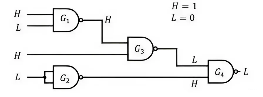
1) \(G_2\)
2) \(G_3\)
3) \(G_4\)
4) \(G_1\)
Check Answer
Option 3
Q.No:33 CSIR Dec-2024
The output of the following circuit is always found to be zero.
Such an observation can be due to
1) Two of the inputs of any one of the NAND gates being accidentally shorted to each other
2) One of the inputs to the NOR gate being accidentally grounded
3) One of the inputs to one of the NAND gates being accidentally grounded
4) Two of the inputs of the NOR gate being accidentally shorted to each other
Check Answer
Option 3
Q.No:34 CSIR Dec-2024
The logic circuit that will have the output
\[
Y = (A + B)\,\overline{(\overline{A}(\overline{B} + \overline{C}))} + \overline{A}(B + C)
\]
is


Check Answer
Option 1
Q.No:35 CSIR June-2025
The minimum number of two-input NOR gates required to obtain the following output for three digital inputs \(A, B, C\)
\[
Y = (\overline{A} + \overline{B} + \overline{C})(\overline{A} + B + \overline{C})(A + \overline{B} + C)
\]
would be
1) 4
2) 3
3) 5
4) 6