
Q.No:1 JEST-2014
Which of the following circuits will act like a 4-input NAND gate?

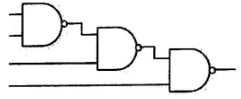


Check Answer
Option d
Q.No:2 JEST-2015
The reference voltage of an analog to digital converter is \(1 V\). The smallest voltage step that the converter can record using a 12-bit converter is,
(a)
\(0.24 V\)
(b)
\(0.24 mV\)
(c)
\(0.24 \mu V\)
(d)
\(0.24 nV\)
Check Answer
Option b
Q.No:3 JEST-2015
For the logic circuit shown in figure 5, the required input condition \((A, B, C)\) to make the output \((X)=1\) is,

(a)
1,0,1
(b)
0,0,1
(c)
1,1,1
(d)
0,1,1
Check Answer
Option d
Q.No:4 JEST-2017
What is \(Y\) for the circuit shown below?

(A)
\(Y=\overline{(A+\bar{B})(\bar{B}+C)}\)
(B)
\(Y=\overline{(A+\bar{B})(B+C)}\)
(C)
\(Y=\overline{(\bar{A}+B)(\bar{B}+C)}\)
(D)
\(Y=\overline{(A+B)(\bar{B}+C)}\)
Check Answer
Option A
Q.No:5 JEST-2020
A 16-bit analog to digital converter works in the range 0-1 Volt. The least count of the converter is
(A)
\(0.3 mV\)
(B)
\(15.26 mV\)
(C)
\(5.44 nV\)
(D)
\(15.26 \mu V\)
Check Answer
Option D
Q.No:6 JEST-2020
The 2's compliment of 1111 1111 is
(A)
0000 0001
(B)
0000 0000
(C)
1111 1111
(D)
1000 0000
Check Answer
Option A
Q.No:7 JEST-2021
A negative logic is the one in which the 0's and the 1's in the truth tables are interchanged. In such a negative logic, the normal NAND gate would behave like a
(A)
NOR gate
(B)
AND gate
(C)
OR gate
(D)
NAND gate
Check Answer
Option A
Q.No:8 JEST-2022
A 12-bit analog-to-digital converter has an operating range of \(0\) to \(1 V\). The smallest voltage step (in mV, upto two significant digits) that one can record using this converter is
Check Answer
Ans 0.24
Q.No:9 JEST-2023
Consider all possible Boolean logic gates with 2 inputs and one output. How many such gates can be constructed?
(a) 16
(b) 4
(c) 2
(d) 8
Check Answer
option a
Q.No:10 JEST-2023
What is the 2's complement representation of 11010110 ?
(a) 11010101
(b) 00101001
(c) 00101010
(d) 01101011
Check Answer
option c
Q.No:11 JEST-2023
Convert the octal number \(3720_8\) to its decimal equivalent.
(a) \(1000_{10}\)
(b) \(2000_{10}\)
(c) \(2020_{10}\)
(d) \(1900_{10}\)
Check Answer
option b
Q.No:12 JEST-2024
What is the output of the following logic circuit?

(a) \( X = A \) AND \( B \) AND \({C} \)
(b) \( X = (A \) OR \( C) \) AND \( (B \) OR \( C) \)
(c) \( X = (A \) OR \( C) \) AND \( (B \) OR \( C) \) AND \( C \)
(d) \( X = (\overline{A} \) OR \( \overline{B} \) OR \( \overline{C}) \) AND \( C \)
This question is withdrawn since the labels are not shown in the figure. ALL CANDIDATES WILL BE AWARDED 3 MARKS.
Check Answer
option a
Q.No:13 JEST-2025
For the logic circuit and the inputs \(P\) and \(Q\) shown in the figure,
which of the following is the correct output \(Y\)?
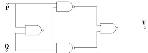


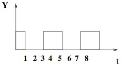

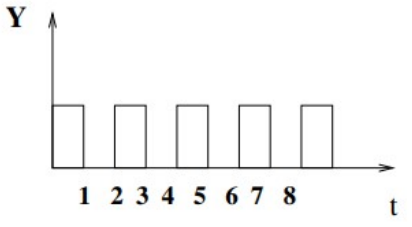
Check Answer
option b
Q.No:1 TIFR-2012
Consider the circuit shown below.

The minimum number of NAND gates required to design this circuit is
(a)
\(6\)
(b)
\(5\)
(c)
\(4\)
(d)
\(3\)
Check Answer
Option c
Q.No:2 TIFR-2013
The circuit shown below uses only NAND gates. Find the final output.
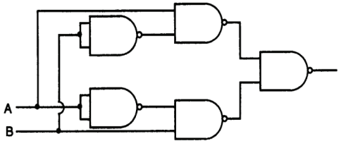
(a)
A XOR B
(b)
A OR B
(c)
A AND B
(d)
A NOR B
Check Answer
Option a
Q.No:3 TIFR-2014
A control circuit needs to be designed to save on power consumption by an air-conditioning unit \(A\) in a windowless room with a single door. The room is fitted with the following devices:
(1)
a temperature sensor \(T\), which is enabled (\(T=1\)) whenever the temperature falls below a pre-set value;
(2)
a humidity sensor \(H\), which is enabled (\(H=1\)) whenever the humidity falls below a certain pre-set value;
(3)
a sensor \(D\) on the door, which is triggered (\(D=1\)) whenever the door opens.
Which of the following logical circuits will turn the air-conditioning unit off (\(A=0\)) whenever the door is opened or when both temperature and humidity are below their pre-set values?

Check Answer
Option c
Q.No:4 TIFR-2015
To measure the voltage in the range \(0\)--\(5 V\) with a precision of \(5 mV\), the minimum number of bits required in a digital voltmeter is
(a)
\(9\)
(b)
\(10\)
(c)
\(11\)
(d)
\(12\)
Check Answer
Option b
Q.No:5 TIFR-2015
A building has three overhead water tanks, each fitted with a sensor (\(S_1, S_2, S_3\)) which goes to \(0\) when the water level in the tank falls below a set value and remains \(1\) otherwise. A common pump is used to raise water from an underground storage tank to these overhead tanks. Of the following circuits, which one will turn on (\(P=1\)) the pump only when at least \(\underline{two}\) of the tanks have water level below the set value?

Check Answer
Option d
Q.No:6 TIFR-2016
In a digital circuit for three input signals (A, B and C) the final output (Y) should be such that for inputs

the output (Y) should be low and for all other cases it should be high.
Which of the following digital circuits will give such output?

Check Answer
Option d
Q.No:7 TIFR-2017
The output (Y) of the following circuit will be

(a)
\(\bar{A}+B+\bar{C}\)
(b)
\(\bar{A}\)
(c)
\(\bar{B}\)
(d)
\(\bar{C}\)
Check Answer
Option d
Q.No:8 TIFR-2017
For exact calculation and minimum complexity, two four-digit binary numbers can be added with
(a)
1 full adder and 3 half-adders
(b)
2 full adders and 2 half-adders
(c)
3 full adders and 1 half-adder
(d)
4 full adders
Check Answer
Option c
Q.No:9 TIFR-2018
In Boolean terms, \((A+B)(A+C)\) is equal to
(a)
\(ABC\)
(b)
\((A+B+C)(A+B)\)
(c)
\(A(B+C)\)
(d)
\(A+BC\)
Check Answer
Option d
Q.No:10 TIFR-2019
The circuit shown below uses only NAND gates.

The final output at {\bf C} is
(a)
\({\bf A}\) AND \({\bf B}\)
(b)
\({\bf A}\) OR \({\bf B}\)
(c)
\({\bf A}\) XOR \({\bf B}\)
(d)
\({\bf A}\) NOR \({\bf B}\)
Check Answer
Option c
Q.No:11 TIFR-2020
An OR gate, a NOR gate and an XOR gate are to be constructed using only NAND gates.
If the minimum number of NAND gates needed to construct OR, NOR and XOR gates is denoted \(n(\text{OR}), n(\text{NOR})\) and \(n(\text{XOR})\) respectively, then
(a)
\(n(\text{NOR})=n(\text{XOR})>n(\text{OR})\)
(b)
\(n(\text{NOR})=n(\text{XOR})=n(\text{OR})\)
(c)
\(n(\text{NOR})>n(\text{XOR})>n(\text{OR})\)
(d)
\(n(\text{NOR})<n(\text{XOR})=n(\text{OR})\)
Check Answer
Option a
Q.No:12 TIFR-2021
A three variable (A, B, C) truth table has a high output for the input conditions 000, 010, 100, and 110 and low otherwise. This effectively means the circuit following this truth table is the equivalent of
(a)
\(\bar{C}\)
(b)
\(A+\bar{A}\)
(c)
\(A+B\)
(d)
\(\bar{C}(A+B)\)
Check Answer
Option a
Q.No:13 TIFR-2021
A sealed box containing a digital circuit has a circuit diagram pasted on its lid as shown below.
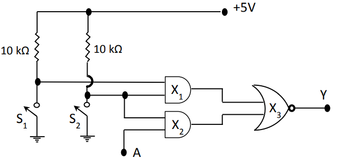
However, the output of the circuit is not as per this diagram. Some of the outputs actually obtained were as shown below

Based on this we can conclude that the actual circuit inside has
(a)
OR gates instead of AND gates (\(X_1\) and \(X_2\))
(b)
NAND gate instead of NOR gate (\(X_3\))
(c)
OR gate instead of NOR gate (\(X_3\))
(d)
AND gate instead of NOR gate (\(X_3\))
Check Answer
Option a
Q.No:14 TIFR-2023
The pulse train at the output of an XNOR gate with the three inputs
\[A=00011011 \]
\[B=10100011\]
\[C=00101110\]
will be
(a)
10010110
(b)
01010111
(c)
01101001
(d)
10101000
Check Answer
Option c
Q.No:15 TIFR-2023
A half-adder circuit is defined as a two-input, two-output logic circuit where the output \(S\) gives the sum of inputs up to a single bit, and the output \(C\) gives carryover in a single bit.
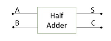
The expected truth table of the half-adder is given as

Which one of the following circuit \(\textbf{does NOT}\) behave like a half-adder?

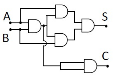


Check Answer
Option b
Q.No:16 TIFR-2024
The minimum number of two input NAND gates required to obtain the output \( Y = \overline{A}B + \overline{C} \) from three inputs \( A \), \( B \) and \( C \) is:
(a) 3
(b) 7
(c) 4
(d) 6
(a) 3
(b) 7
(c) 4
(d) 6
Check Answer
Option a
Q.No:17 TIFR-2024
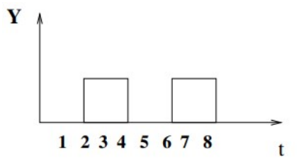
A technician receives an electronic instrument on which the following circuit diagram is drawn. Based on the shown timing diagram (binary values at pins 1, 2, 3, 4, 5 as a function of time) measured by the technician, identify the fault in the instrument.
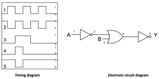
(a) An AND gate is used where an OR gate should have been used
(b) Input inverter acts like an OR gate
(c) Pin 4 shorted to ground
(d) Output inverter is faulty
Check Answer
Option a
Q.No:18 TIFR-2025
The output pulse train \(Y\) of the circuit shown on the right, with three
synchronized input trains,
\[A = 00001111\]
\[B = 00110011\]
\[C = 01010101\]
will be:
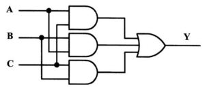
a) 00010111
b) 00100111
c) 01010101
d) 00010001