
Q.No:1 CSIR Dec-2014
The \(I\)-\(V\) characteristics of the diode in the circuit below is given by
\[
I=
\left\{
\begin{array}{ll}
(V-0.7)/500 & \text{for }V\geq 0.7 \\
0 & \text{for }V<0.7
\end{array}
\right.
\]
where \(V\) is measured in volts and \(I\) is measured in amperes.
The current \(I\) is the circuit is
(1)
\(10.0 mA\)
(2)
\(9.3 mA\)
(3)
\(6.2 mA\)
(4)
\(6.7 mA\)
Check Answer
Option 3
Q.No:2 CSIR Dec-2016
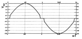
The \(I\)-\(V\) characteristics of a device is \(I=I_s\left[\exp{\left(\frac{aV}{T}\right)}-1\right]\), where \(T\) is the temperature and \(a\) and \(I_s\) are constants independent of \(T\) and \(V\). Which one of the following plots is correct for a fixed applied voltage \(V\)?


Check Answer
Option 4
Q.No:3 CSIR June-2017
Let \(I_0\) be the saturation current, \(\eta\) the ideality factor and \(v_F\) and \(v_R\) the forward and reverse potentials, respectively, for a diode. The ratio \(R_R/R_F\) of its reverse and forward resistances \(R_R\) and \(R_F\) respectively, varies as (In the following \(k_B\) is the Boltzmann constant, \(T\) is the absolute temperature and \(q\) is the charge.)
(1)
\(\frac{v_R}{v_F}\exp{\left(\frac{qv_F}{\eta k_B T}\right)}\)
(2)
\(\frac{v_F}{v_R}\exp{\left(\frac{qv_F}{\eta k_B T}\right)}\)
(3)
\(\frac{v_R}{v_F}\exp{\left(-\frac{qv_F}{\eta k_B T}\right)}\)
(4)
\(\frac{v_F}{v_R}\exp{\left(-\frac{qv_F}{\eta k_B T}\right)}\)
Check Answer
Option 1
Q.No:4 CSIR Dec-2017
A Zener diode with an operating voltage of \(10 V\) at \(25^{\circ}C\) has a positive temperature coefficient of \(0.07\%\) per \({}^{\circ}C\) of the operating voltage. The operating voltage of this Zener diode at \(125^{\circ}C\) is
(1)
\(12.0 V\)
(2)
\(11.7 V\)
(3)
\(10.7 V\)
(4)
\(9.3 V\)
Check Answer
Option 3
Q.No:5 CSIR Dec-2017
In the circuit below, \(D_1\) and \(D_2\) are two silicon diodes with the same characteristics. If the forward voltage drop of a silicon diode is \(0.7 V\), then the value of the current \(I_1+I_{D_1}\) is

(1)
\(18.6 mA\)
(2)
\(9.3 mA\)
(3)
\(13.95 mA\)
(4)
\(14.65 mA\)
Check Answer
Option 3
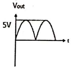
Q.No:6 CSIR June-2018
A sinusoidal signal with a peak voltage \(V_P\) and average value zero, is an input to the following circuit.

Assuming ideal diodes, the peak value of the output voltage across the load resistor \(R_L\), is
(1)
\(V_P\)
(2)
\(V_P/2\)
(3)
\(2V_P\)
(4)
\(\sqrt{2}V_P\)
Check Answer
Option 3
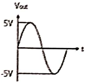
Q.No:7 CSIR Dec-2018
A sinusoidal voltage having a peak value of \(V_P\) is an input to the following circuit, in which the DC voltage is \(V_b\).

Assuming an ideal diode, which of the following best describes the output waveform?


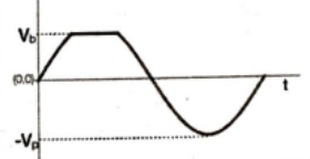

Check Answer
Option 3
Q.No:1X CSIR Dec-2018
In the circuit below, \(D\) is an ideal diode, the source voltage \(V_S=V_0\sin{\omega t}\) is a unit amplitude sine wave and \(R_S=R_L\)

The average output voltage, \(V_L\), across the load resistor \(R_L\) is
1. \(\frac{1}{2\pi}V_0\)
2. \(\frac{3}{2\pi}V_0\)
3. \(3V_0\)
4. \(V_0\)
Check Answer
Option a
Q.No:8 CSIR June-2020
Two voltmeters \(A\) and \(B\) with internal resistances \(2 M\Omega\) and \(0.1 k\Omega\) are used to measure the voltage drops \(V_A\) and \(V_B\), respectively, across the resistor \(R\) in the circuit shown below.

The ratio \(V_A/V_B\) is
(a)
\(0.58\)
(b)
\(1.73\)
(c)
\(1\)
(d)
\(2\)
Check Answer
Option b
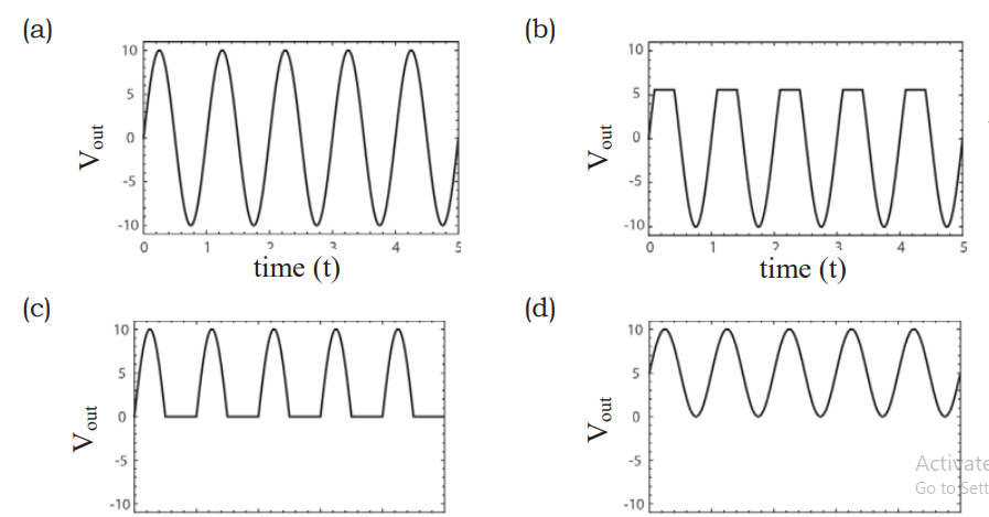
Q.No:9 CSIR Sep-2022
A high impedance load (network) is connected in the circuit as shown below.
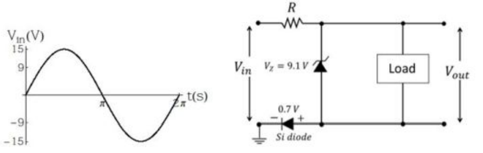
The forward voltage drop for silicon diode is 0.7 V and Zener voltage 9.10 V. If the input voltage \((V_{in})\) is sine wave with an amplitude of 15 V (as shown in the figure above) , which one of the following waveform qualitatively describes the output voltage \((V_{out})\) across the load ?
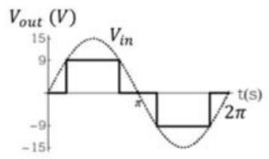
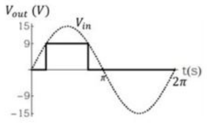
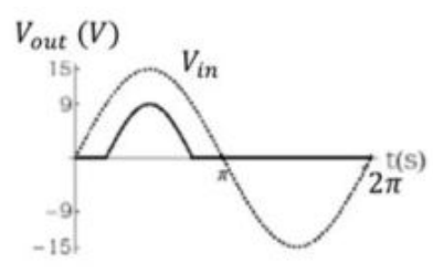
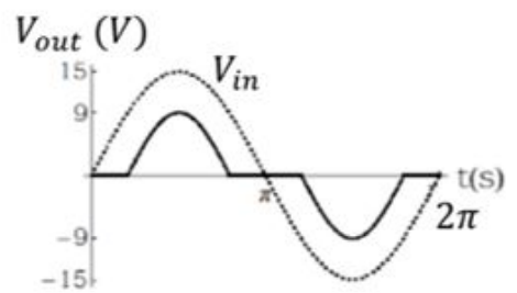
Check Answer
Option 2
Q.No:10 CSIR JUNE-2023
In the circuit shown below, four silicon diodes and four capacitors are connected to a sinusoidal voltage source of amplitude \(V_{in}>0.7\hspace{1mm}V\) and frequency \(1\) kHz. If the knee voltage for each of the diodes is \(0.7 \hspace{1mm}V\) and the resistances of the capacitors are negligible, the DC output voltage \(V_{out}\) after \(2\) seconds of strating the voltage source is closest to

1) \(4V_{in}-0.7\hspace{1mm}V\)
2) \(4V_{in}-2.8\hspace{1mm}V\)
3) \(V_{in}-0.7\hspace{1mm}V\)
4) \(V_{in}-2.8\hspace{1mm}V\)
Check Answer
Option 2
Q.No:11 CSIR JUNE-2025
A silicon p–n junction diode is operated under forward bias at two temperatures
\(T_{\text{hi}} \approx 300\ \text{K}\) (shown by solid line) and
\(T_{\text{lo}} \approx 200\ \text{K}\) (shown by dotted line).
Which of the following plots best represents the I–V characteristics of the diode?
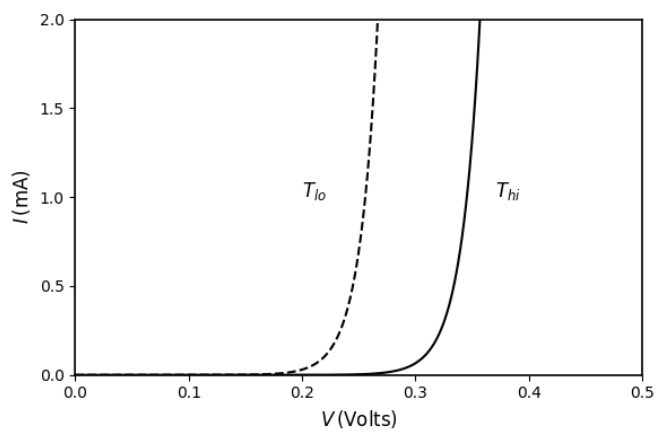

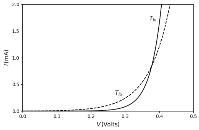
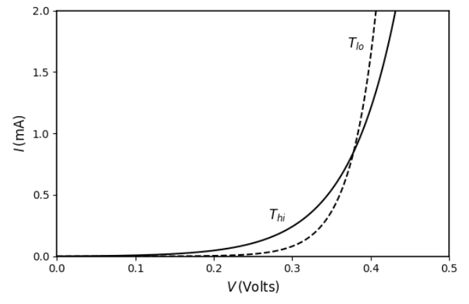
Check Answer
Option 2
Q.No:1 GATE-2012
If the peak output voltage of a full wave rectifier is \(10 V\), its d.c. voltage is
(A)
\(10.0 V\)
(B)
\(7.07 V\)
(C)
\(6.36 V\)
(D)
\(3.18 V\)
Check Answer
Option C
Q.No:2 GATE-2012
In the following circuit, the voltage drop across the ideal diode in forward bias condition is \(0.7 V\)

The current passing through the diode is
(A)
\(0.5 mA\)
(B)
\(1.0 mA\)
(C)
\(1.5 mA\)
(D)
\(2.0 mA\)
Check Answer
Option B
Q.No:3 GATE-2017
In the figure given below, the input to the primary of the transformer is a voltage varying sinusoidally with time. The resistor \(R\) is connected to the centre tap of the secondary. Which one of the following plots represents the voltage across the resistor \(R\) as a function of time?


Check Answer
Option A
Q.No:4 GATE-2020
Consider the circuit given in the figure. Let the forward voltage drop across each diode be \(0.7 V\). The current \(I\) (in mA) through the resistor is _____________.

Check Answer
Ans 8
Q.No:5 GATE-2022
For a bipolar junction transistor, which of the following statements are true?
(a)
Doping concentration of emitter region is more than that in collector and base region
(b)
Only electrons participate in current conduction
(c)
The current gain \(\beta\) depends on temperature
(d)
Collector current is less than the emitter current
Check Answer
Option a,c,d
Q.No:6 GATE-2023
Choose the most appropriate matching of the items in Column 1 with those in Column 2.
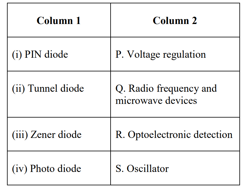
(A)
(i) - Q; (ii) - S; (iii) - P; (iv) - R
(B)
(i) - R; (ii) - Q; (iii) - P; (iv) - S
(C)
(i) - R; (ii) - S; (iii) - P; (iv) - Q
(D)
(i) - P; (ii) - Q; (iii) - R; (iv) - S
Check Answer
Option A
Q.No:7 GATE-2024
The symbols \( C \), \( D \), \( V_{in} \) and \( V_{o} \) shown in the figure denote capacitor, ideal diode, input voltage and output voltage, respectively.
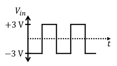
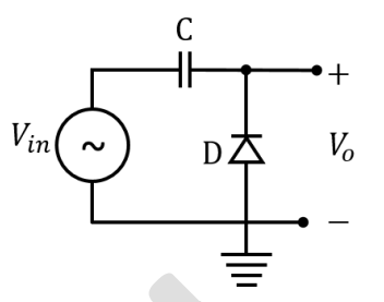
Which one of the following output waveforms (\( V_{o} \)) is correct for the given input waveform (\( V_{in} \))?

Check Answer
Option A
Q.No:1 JEST-2017
In the following silicon diode circuit (\(V_B=0.7 V\)), determine the output voltage waveform (\(V_{out}\)) for the given input wave.


Check Answer
Option B
Q.No:2 JEST-2017
Consider the circuit shown in the figure where \(R_1=2.07 k\Omega\) and \(R_2=1.93 k\Omega\). Current source \(I\) delivers \(10 mA\) current. The potential across the diode \(D\) is \(0.7 V\). What is the potential at \(A\)?

(A)
\(10.35 V\)
(B)
\(9.65 V\)
(C)
\(19.30 V\)
(D)
\(4.83 V\)
Check Answer
Option B
Q.No:3 JEST-2018
A Germanium diode is operated at a temperature of \(27\) degree C. The diode terminal voltage is \(0.3 V\) when the forward current is \(10 mA\). What is the forward current (in mA) if the terminal voltage is \(0.4 V\)?
(A)
\(477.3\)
(B)
\(577.3\)
(C)
\(47.73\)
(D)
\(57.73\)
Check Answer
Option A
Q.No:4 JEST-2019
The circuit given below is fed by a sinusoidal voltage \(V_{in}=V_0 \sin{\omega t}\). Assume that the cut-in voltage of the diode is \(0.7\) volts and \(V_1\) is a positive dc voltage smaller than \(V_0\). Which one of the following statements is true about \(V_{out}\)?

(A)
Positive part of \(V_{out}\) is restricted to a maximum voltage of \(0.7+\frac{R_2}{R_1+R_2}V_1\)
(B)
Negative part of \(V_{out}\) is restricted to a maximum voltage of \(0.7+\frac{R_2}{R_1+R_2}V_1\)
(C)
Positive part of \(V_{out}\) is restricted to a maximum voltage of \(0.7+\frac{R_1}{R_1+R_2}V_1\)
(D)
Negative part of \(V_{out}\) is restricted to a maximum voltage of \(0.7+\frac{R_1}{R_1+R_2}V_1\)
Check Answer
Option A
Q.No:5 JEST-2021
In an open circuited p-n junction diode, the barrier voltage at the junction is generated due to
(A)
Minority carriers in the p and n sides
(B)
Majority carriers in the p and n sides
(C)
Immobile negative charge in the p-side and positive charge in the n-side
(D)
Immobile positive charge in the p-side and negative charge in the n-side
Check Answer
Option C
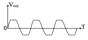
Q.No:6 JEST-2021
The circuit given in the figure below is composed of ideal diodes and resistances \(R\). The input waveform is shown on the left.

The output waveform would be


Check Answer
Option A
Q.No:7 JEST-2021
What is the output waveform of the circuit for the given input signal? Assume that the zener diodes are identical, amplitude of the input voltage \( V_{in} \) is twice the zener breakdown voltage, and \( R_L = 10R \).

Check Answer
Option A
Q.No:8 JEST-2025
A silicon p–n junction diode operates at \(27^\circ\text{C}\).
The current \(I\) is doubled when the forward bias is increased.
[Assume \(I \gg I_s\), where \(I_s\) is the reverse saturation current,
and the emission coefficient \(\eta_{Si} = 2\)].
The increase in the forward bias is closest to:
A) 54 mV
B) 36 mV
C) 18 mV
D) 72 mV
Check Answer
Option B
Q.No:1 TIFR-2012
The voltage regulator circuit shown in the figure has been made with a Zener diode rated at \(15 V, 200 mW\). It is required that the circuit should dissipate \(150 mW\) power across the fixed load resistor \(R_L\).

For stable operation of this circuit, the input voltage \(V_i\) must have a range
(a)
\(17.5 V\)--\(20.5 V\)
(b)
\(15.5 V\)--\(20.5 V\)
(c)
\(15.5 V\)--\(22.5 V\)
(d)
\(17.5 V\)--\(22.5 V\)
(e)
\(15.0 V\)--\(22.5 V\)
Check Answer
Option a
Q.No:2 TIFR-2013
The figure on the right shows the current-voltage characteristics of a diode over a range of voltage and current where it is safe to operate the diode.

When this diode is used in the circuit on the extreme right, the approximate current, in mA, through the diode will be
(a)
\(0\)
(b)
\(8.3\)
(c)
\(16.7\)
(d)
\(25\)
Check Answer
Option b
Q.No:3 TIFR-2014
Consider the following circuit.

Which of the graphs given below is a correct representation of \(V_{\text{out}}\)?
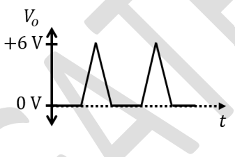
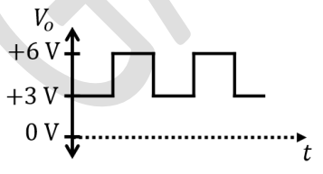
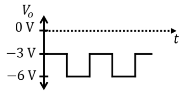
Check Answer
Option b
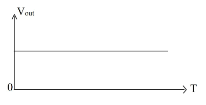
Q.No:4 TIFR-2019
The signal shown on the left side of the figure below is fed into the circuit shown on the right side.

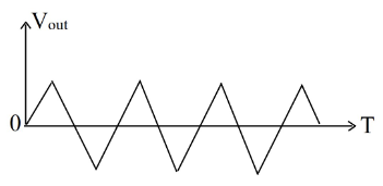
If the signal has time period \(\tau_S\) and the circuit has a natural frequency \(\tau_{RC}\), then, in the case when \(\tau_S\ll \tau_{RC}\), the steady-state output will resemble

Check Answer
Option d
Q.No:5 TIFR-2019
Drawing power from a \(12 \hspace{1mm}\text{V}\) car battery, a \(9 \hspace{1mm}\text{V}\) stabilized DC voltage is required to power a car stereo system, attached to the terminals A and B, as shown in the figure.
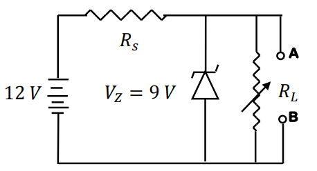
If a Zener diode with ratings, \(V_Z=9\hspace{1mm}\text{V}\) and \(P_{\text{max}}=0.27\hspace{1mm}\text{W}\), is connected as shown in the figure, for the above purpose, the minimum series resistance \(R_S\) must be
(a)
\(111\hspace{1mm}\Omega\)
(b)
\(103\hspace{1mm}\Omega\)
(c)
\(100\hspace{1mm}\Omega\)
(d)
\(97\hspace{1mm}\Omega\)