
CAUTION : Try solving the problem yourself for at least 5–10 minutes before clicking the AI Assistant. In the exam hall, you will be on your own.
Q.No:1 CSIR Dec-2014
Consider the amplifier circuit comprising of the two op-amps \(A_1\) and \(A_2\) as shown in the figure.

If the input ac signal source has an impedance of \(50 k\Omega\), which of the following statements is true?
(1)
\(A_1\) is required in the circuit because the source impedance is much greater than \(r\)
(2)
\(A_1\) is required in the circuit because the source impedance is much less than \(R\)
(3)
\(A_1\) can be eliminated from the circuit without affecting the overall gain
(4)
\(A_1\) is required in the circuit if the output has to follow the phase of the input signal
Check Answer
Option 1_3
Q.No:2 CSIR June-2015
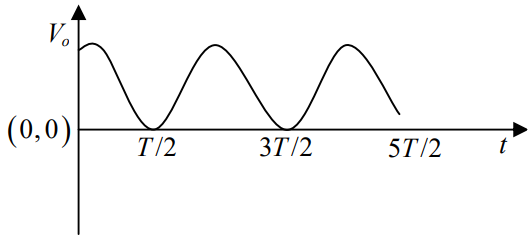
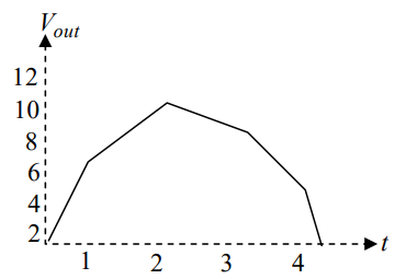
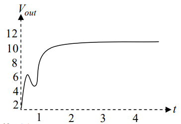
For the circuit and the input sinusoidal waveform shown in the figures below. which is the correct waveform at the output?

(The time scales in all the plots are the same.)


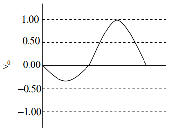
Check Answer
Option 2
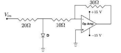
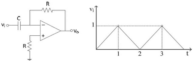
Q.No:3 CSIR June-2015
In the circuit given below, the thermistor has a resistance 3 k\(\Omega\) at 25°C. Its resistance decreases by 150 \(\Omega\) per °C upon heating. The output voltage of the circuit at 30°C is

(1)
\(-3.75 V\)
(2)
\(-2.25 V\)
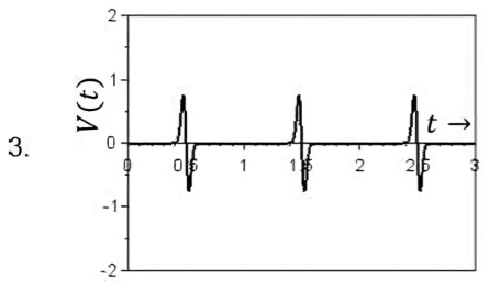
(3)
\(2.25 V\)
(4)
\(3.75 V\)
Check Answer
Option 3
Q.No:4 CSIR Dec-2015
If the parameters \(y\) and \(x\) are related by \(y=\log{(x)}\), then the circuit that can be used to produce an output voltage \(V_0\) varying linearly with \(x\) is


Check Answer
Option 3
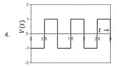
Q.No:5 CSIR June-2016
Given the input voltage \(V_i\), which of the following waveforms correctly represents the output voltage \(V_0\) in the circuit shown below?


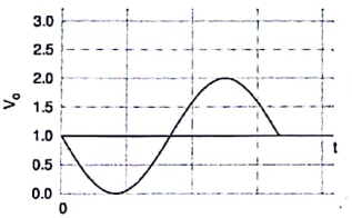


Check Answer
Option 2
Q.No:6 CSIR Dec-2016
In the circuit below, the input voltage \(V_i\) is \(2V\), \(V_{cc}=16 V\), \(R_2=2 k\Omega\) and \(R_L=10 k\Omega\).
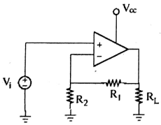
The value of \(R_1\) required to deliver \(10 mW\) of power across \(R_L\) is
(1)
\(12 k\Omega\)
(2)
\(4 k\Omega\)
(3)
\(8 k\Omega\)
(4)
\(14 k\Omega\)
Check Answer
Option 3
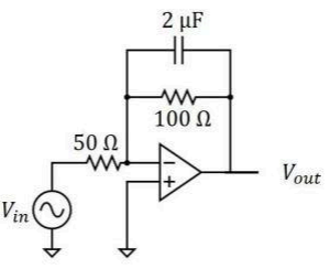
Q.No:7 CSIR June-2017
The gain of the circuit given below is \(-\frac{1}{\omega RC}\).

The modification in the circuit required to introduce a dc feedback is to add a resistor
(1)
between a and b
(2)
between positive terminal of the op-amp and ground
(3)
in series with \(C\)
(4)
parallel to \(C\)
Check Answer
Option 4
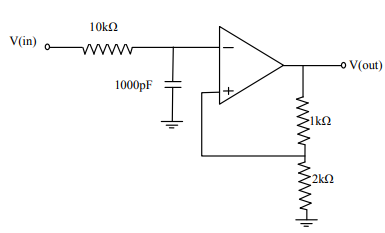
Q.No:8 CSIR June-2017
In the following operational amplifier circuit \(C_{in}=10 nF, R_{in}=20 k\Omega, R_F=200 k\Omega\) and \(C_F=100 pF\).

The magnitude of the gain at a input signal frequency of \(16 kHz\) is
(1)
\(67\)
(2)
\(0.15\)
(3)
\(0.3\)
(4)
\(3.5\)
Check Answer
Option
Q.No:9 CSIR June-2018
The input \(V_i\) to the following circuit is a square wave as shown in the following figure.

Which of the waveforms \(V_0\) best describes the output?


Check Answer
Option
Q.No:10 CSIR Dec-2018
The input \(V_i\) to the following circuit is a square wave as shown in the following figure.

Which of the waveforms best describes the output?


Check Answer
Option
Q.No:11 CSIR June-2019
The forward diode current is given by \(I=\kappa T^{\alpha} e^{-E_g/k_B T}(\exp{(eV/k_B T)}-1)\), where \(E_g\) is the band gap of the semiconductor, \(V\) is the voltage drop across the diode, \(T\) is the temperature of the diode operating near room temperature and, \(\alpha\) and \(\kappa\) are constants. A diode is used as a thermal sensor in the circuit shown below.

If \(V\) is measured using an ideal voltmeter to estimate \(T\), the variation of the voltage \(V\) as a function of \(T\) is best approximated by (in the following \(a\) and \(b\) are constants)
(1)
\(aT^2+b\)
(2)
\(aT+b\)
(3)
\(aT^3+b\)
(4)
\(aT+bT^2\)
Check Answer
Option 2
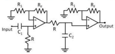
Q.No:12 CSIR June-2019
A circuit constructed using op-amp, resistor \(R_1=1 k\Omega\) and capacitors \(C_1=1 \mu F\) and \(C_2=0.1 \mu F\), is shown in the figure below.

This circuit will act as a
(1)
high pass filter
(2)
low pass filter
(3)
band pass filter
(4)
band reject filter
Check Answer
Option 1
Q.No:13 CSIR Dec-2019
In the circuit below, \(D\) is an ideal diode, the source voltage \(V_S=V_0\sin{\omega t}\) is a unit amplitude sine wave and \(R_S=R_L\)

The average output voltage, \(V_L\), across the load resistor \(R_L\) is
(1)
\(\frac{1}{2\pi}V_0\)
(2)
\(\frac{3}{2\pi}V_0\)
(3)
\(3V_0\)
(4)
\(V_0\)
Check Answer
Option 1
Q.No:14 CSIR Dec-2019
In the circuit diagram of a band pass filter shown below, \(R=10 k\Omega\).
In order to get a lower cut-off frequency of \(150 Hz\) and an upper cut-off frequency of \(10 kHz\), the appropriate values of \(C_1\) and \(C_2\) respectively are
(1)
\(0.1 \mu F\) and \(1.5 nF\)
(2)
\(0.3 \mu F\) and \(5.0 nF\)
(3)
\(1.5 nF\) and \(0.1 \mu F\)
(4)
\(5.0 nF\) and \(0.3 \mu F\)
Check Answer
Option 1
Q.No:15 Assam CSIR Dec-2019
The sinusoidal input (in figure A) is applied to the circuit (in figure B), with \(R_1/R_2\) such that the Op-amp is driven to saturation.

The maximum possible value of the output voltage (\(V_{out}\)) is closest is
(1)
\(V/\sqrt{2}\)
(2)
\(V\)
(3)
\(V/2\)
(4)
\(2V\)
Check Answer
Option 3
Q.No:16 Assam CSIR Dec-2019
In the circuit shown in the figure below, \(V_1(t)=50\sin{(1000t)} mV\) and \(V_2(t)=10\sin{(3000t)} mV\). The cut-off frequency of the low pass filter is \(200 Hz\).

The frequency of the output voltage \(V_0(t)\) is closest to
(1)
\(100 Hz\)
(2)
\(130 Hz\)
(3)
\(160 Hz\)
(4)
\(190 Hz\)
Check Answer
Option 3
Q.No:17 CSIR June-2020
The \(I\)-\(V\) characteristics of the diode \(D\) in the circuit below is given by
\[
I=I_S\left(e^{\frac{qV}{k_B T}}-1\right)
\]
where \(I_S\) is the reverse saturation current, \(V\) is the voltage across the diode and \(T\) is the absolute temperature.

If the input voltage is \(V_{in}\), then the output voltage \(V_{out}\) is
(a)
\(I_S R\ln{\left(\frac{qV_{in}}{k_B T}+1\right)}\)
(b)
\(\frac{1}{q}k_B T\ln{\left(\frac{q(V_{in}+I_S R)}{k_B T}\right)}\)
(c)
\(\frac{1}{q}k_B T\ln{\left(\frac{V_{in}}{I_S R}+1\right)}\)
(d)
\(-\frac{1}{q}k_B T\ln{\left(\frac{V_{in}}{I_S R}+1\right)}\)
Check Answer
Option c
Q.No:18 CSIR June-2020
In the circuit shown below, the gain of the op-amp in the middle of its bandwidth is \(10^5\). A sinusoidal voltage with angular frequency \(\omega=100 rad/s\) is applied to the input of the op-amp.

The phase difference between the input and the output voltage is
(a)
\(5\pi/4\)
(b)
\(3\pi/4\)
(c)
\(\pi/2\)
(d)
\(\pi\)
Check Answer
Option a
Q.No:19 CSIR Feb-2022
The pressure of a gas in a vessel needs be maintained between \(1.5\) bar to \(2.5\) bar in an
experiment. The vessel is fitted with a pressure transducer that generates \(4\)mA to \(20\)mA current
for pressure in the range 1 bar to 5 bar. The current output of the transducer has a linear
dependence on the pressure.
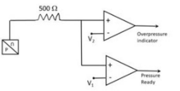
The reference voltages \(V_1\) and \(V_2\) in the comparators in the circuit (shown in figure above)
suitable for the desired operating conditions are respectively
(1)
\(2\)V and \(10\) V
(2)
\(2\)V and \(5\) V
(3)
\(3\)V and \(10\) V
(4)
\(3\)V and \(5\) V
Check Answer
Option 4
Q.No:20 CSIR Feb-2022
In the following circuit the input voltage \(V_{in}\) is such that \(|V_{in}|<|V_{sat}|\) where \(V_{sat}\) is the
saturation voltage of the op-amp (Assume that the diode is an ideal one and \(R_LC\) is much larger
than the duration of the measurement.)

For the input voltage as shown in the figure above the output voltage \(V_{out}\) is best represented by

Check Answer
Option 1
Q.No:21 CSIR Sep-2022
An amplifier with a voltage gain of 40 dB without feedback is used in an electronic circuit. A negative feedback with a
fraction 1/40 is connected to the input of this amplifier. The net gain of the amplifier in the circuit is closest to
(1)
40 dB
(2)
37 dB
(3)
29 dB
(4)
20 dB
Check Answer
Option 3
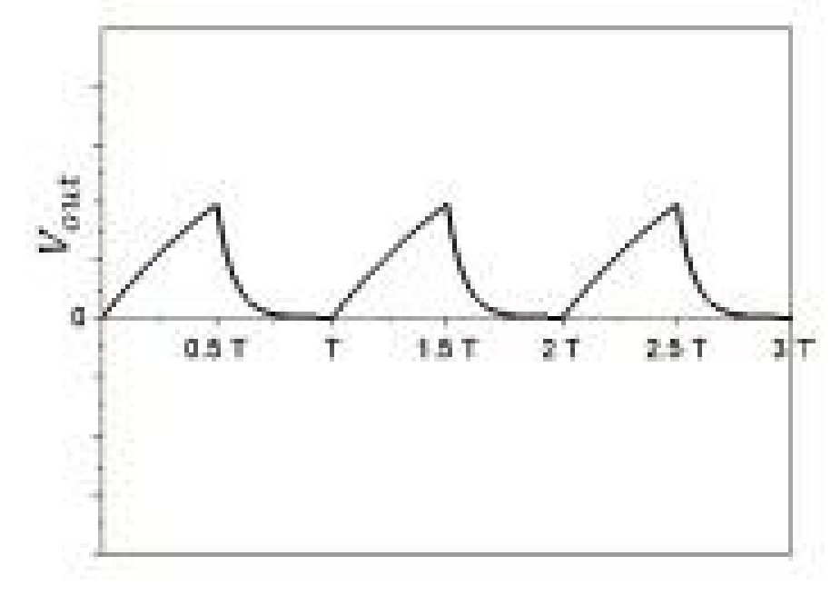
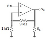
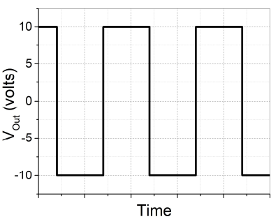
Q.No:22 CSIR June-2023
In the circuit below, there is a voltage drop of \(0.7 \hspace{1mm} V\) across the diode \(D\) in forward bias, while no current flows through it in reverse bias.
If \(V_{in}\) is a sinusoidal signal of frequency \(50 \hspace{1mm} Hz\) with an RSM value of \(1 \hspace{1mm} V\), the maximum current that flows through the diode is closest to
1) \(1 \hspace{1mm}A\)
2) \(0.14 \hspace{1mm}A\)
3) \(0 \hspace{1mm}A\)
4) \(0.07 \hspace{1mm}A\)
Check Answer
Option 3
Q.No:23 CSIR Dec-2023
A circuit with operational amplifier is shown in the figure below.

The output voltage waveform \(V_{out}\) will be closest to


Check Answer
Option A
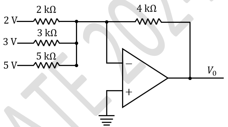
Q.No:24 CSIR Dec-2023
In the circuit shown below using an ideal opamp, inputs \( V_j \) (j = 1, 2, 3, 4) may either be open or connected to a \( -5 V\) battery.

The minimum measurement range of a voltmeter to measure all possible values of \( V_{\text{out}} \) is
1) 10 V
2) 30 V
3) 3 V
4) 1 V
Check Answer
Option 1
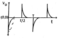
Q.No:25 CSIR June-2024
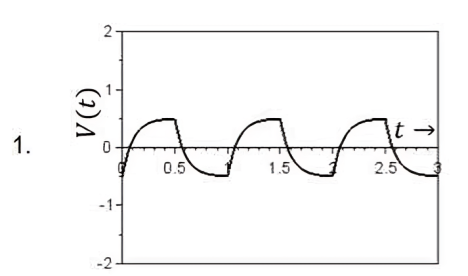
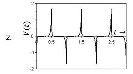
A train of square wave pulses is given to the input of an ideal opamp circuit shown below.
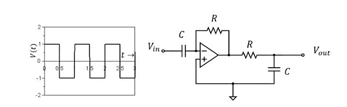
Given that the time period of the input pulses \( T \ll RC \) and the opamp does not get into saturation, which of the following best represents the output waveform?
Check Answer
Option 4
Q.No:26 CSIR Dec-2024
In the circuit shown below, the input voltage (in volts) is given by
\[
V_{\text{in}}(t) = 0.1 \sin(\omega_1 t) + \sin(\omega_2 t),
\]
where
\[
\omega_1 = 5 \times 10^{2}\ \text{s}^{-1}, \qquad
\omega_2 = 5 \times 10^{4}\ \text{s}^{-1}.
\]
The time-varying part of the output voltage \(V_{\text{out}}(t)\) (in volts) is
closest to
1) \(-0.2 \sin(\omega_1 t) - 2 \sin(\omega_2 t)\)
2) \(-0.2 \sin(\omega_1 t) + 0.2 \cos(\omega_2 t)\)
3) \(2 \cos(\omega_1 t) + 0.2 \cos(\omega_2 t)\)
4) \(2 \cos(\omega_1 t) - 2 \sin(\omega_2 t)\)
Check Answer
Option 2
Q.No:1 GATE-2012
Consider the following OP-AMP circuit.

Which one of the following correctly represents the output \(V_{\text{out}}\) corresponding to the input \(V_{\text{in}}\)?


Check Answer
Option A
Q.No:2 GATE-2012
In the following circuit, for the output voltage to be \(V_0=(-V_1+V_2/2)\), the ratio \(R_1/R_2\) is

(A)
\(1/2\)
(B)
\(1\)
(C)
\(2\)
(D)
\(3\)
Check Answer
Option D
Q.No:3 GATE-2013
Consider the following circuit

For this circuit the frequency above which the gain will decrease by \(20 dB\) per decade is
(A)
\(15.9 kHz\)
(B)
\(1.2 kHz\)
(C)
\(5.6 kHz\)
(D)
\(22.5 kHz\)
Check Answer
Option A
Q.No:4 GATE-2013
Consider the following circuit
At \(1.2 kHz\) the closed loop gain is
(A)
\(1\)
(B)
\(1.5\)
(C)
\(3\)
(D)
\(0.5\)
Check Answer
Option B
Q.No:5 GATE-2014
The input given to an ideal OP-AMP integrator circuit is

The correct output of the integrator circuit is


Check Answer
Option A
Q.No:6 GATE-2014
A low pass filter is formed by a resistance \(R\) and a capacitance \(C\). At the cut-off angular frequency \(\omega_c=\frac{1}{RC}\), the voltage gain and the phase of the output voltage relative to the input voltage respectively, are
(A)
\(0.71\) and \(45^{\circ}\)
(B)
\(0.71\) and \(-45^{\circ}\)
(C)
\(0.5\) and \(-90^{\circ}\)
(D)
\(0.5\) and \(90^{\circ}\)
Check Answer
Option B
Q.No:7 GATE-2015
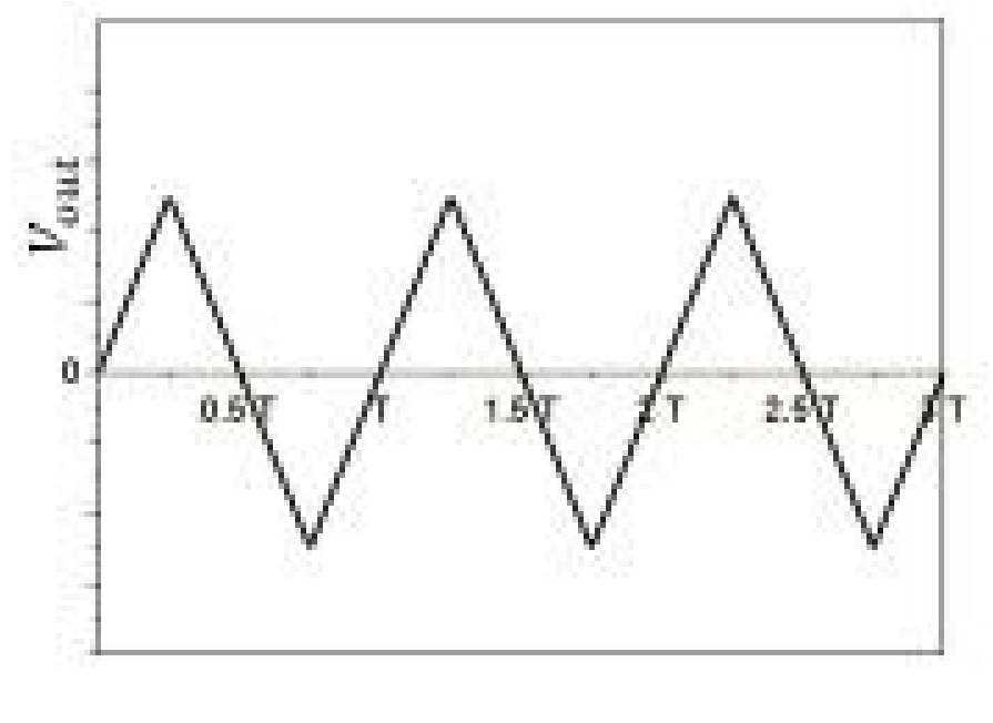
Consider the circuit shown in the figure, where \(RC=1\). For an input signal \(V_i\) shown below, choose the correct \(V_0\) from the options:


Check Answer
Option B
Q.No:8 GATE-2015
In the given circuit, if the open loop gain \(A=10^5\), the feedback configuration and the closed loop gain \(A_f\) are
(A)
series-shunt, \(A_f=9\)
(B)
series-series, \(A_f=10\)
(C)
series-shunt, \(A_f=10\)
(D)
series-shunt, \(A_f=10\)
Check Answer
Option C
Q.No:9 GATE-2017
Consider an ideal operational amplifier as shown in the figure below with \(R_1=5 k\Omega, R_2=1 k\Omega, R_L=100 k\Omega\). For an applied input voltage \(V=10 mV\), the current passing through \(R_2\) is __________. \(\mu A\). (up to two decimal places).

Check Answer
Ans 9.80-10.20
Q.No:10 GATE-2018
For an operational amplifier (ideal) circuit shown below,

if \(V_1=1 V\) and \(V_2=2 V\), the value of \(V_0\) is________________. V (up to one decimal place).
Check Answer
Ans (-3.7 TO -3.5)
Q.No:11 GATE-2019
For the following circuit, what is the magnitude of \(V_{\text{out}}\) if \(V_{\text{in}}=1.5 V\)?

(A)
\(0.015 V\)
(B)
\(0.15 V\)
(C)
\(15 V\)
(D)
\(150 V\)
Check Answer
Option C
Q.No:12 GATE-2020
The input voltage (\(V_{\text{in}}\)) to the circuit shown in the figure is \(2\cos{(100t)} V\). The output voltage (\(V_{\text{out}}\)) is \(2\cos{(100t-\frac{\pi}{2})} V\). If \(R=1 k\Omega\), the value of \(C\) (in \(\mu F\)) is

(A)
\(0.1\)
(B)
\(1\)
(C)
\(10\)
(D)
\(100\)
Check Answer
Option C
Q.No:13 GATE-2022
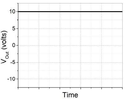
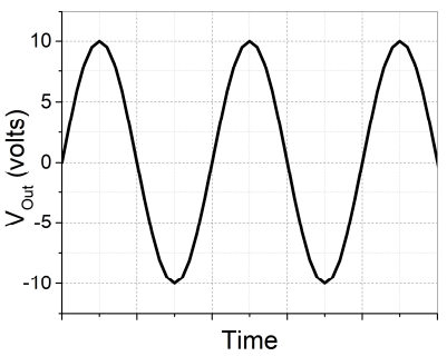
For the Op-Amp circuit shown below, choose the correct output waveform corresponding to the input \(V_{in}=1.5\sin{20\pi t}\) (in Volts). The saturation voltage for this circuit is \(V_{sat}=\pm 10\hspace{1mm}\text{V}\).


Check Answer
Option a
Q.No:14 GATE-2022
For an Op-Amp based negative feedback, non-inverting amplifier, which of the following statements are true?
(a)
Closed loop gain \(<\) Open loop gain
(b)
Closed loop bandwidth \(<\) Open loop bandwidth
(c)
Closed loop input impedance \(>\) Open loop input impedance
(d)
Closed loop output impedance \(<\) Open loop output impedance
Check Answer
Option a,c,d
Q.No:15 GATE-2023
For a transistor amplifier, the frequency response is such that the mid band voltage gain is 200. The cutoff frequencies are 20 Hz and 20 kHz. What is the ratio (rounded off to two decimal places) of the voltage gain at 10 Hz to that at 100 kHz?
Check Answer
Ans 2.20-2.36
Q.No:16 GATE-2024
Consider the operational amplifier circuit shown in figure.
The output voltage \( V_0 \) is ________ V (in integer).
Check Answer
Ans 12
Q.No:17 GATE-2025
The figure shows an op-amp circuit with a 5.1 V Zener diode in the feedback loop.
The op-amp runs from ±15 V supplies.
If a +1 V signal is applied at the input, the output voltage
(rounded off to one decimal place) is
