Q.No:1 JEST-2012
The classic three op-amp instrumentation amplifier configuration is shown below:

The op-amps are ideal and all resistors are of equal value \(R\). The gain, defined as the output voltage \(V_0\) divided by the differential input voltage \(V_1-V_2\), is equal to
(a)
\(2\)
(b)
\(3\)
(c)
\(4\)
(d)
\(6\)
Check Answer
Option b
Q.No:2 JEST-2015
What is the voltage at the output of the following operational amplifier circuit [See in the figure]?
(a)
\(1 V\)
(b)
\(1 mV\)
(c)
\(1 \mu V\)
(d)
\(1 nV\)
Check Answer
Option b
Q.No:3 JEST-2017
Consider a \(741\) operational amplifier circuit as shown below, where \(V_{CC}=V_{EE}=+15 V\) and \(R=2.2 k\Omega\). If \(v_I=2 mV\), what is the value of \(v_O\) with respect to the ground?
(A)
\(-1 mV\)
(B)
\(-2 mV\)
(C)
\(-3 mV\)
(D)
\(-4 mV\)
Check Answer
Option C
Q.No:4 JEST-2019
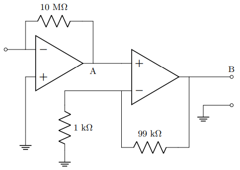
Analyse the ideal op-amp circuit in the figure. Which one of the following statements is true about the output voltage \(V_{out}\), when terminal `C' is connected to point `A' and then to point `B'?

(A)
\(V_{out}=V_{in}\) and \(V_{out}=-V_{in}\) when `C' is connected to `A' and `B', respectively.
(B)
\(V_{out}=-V_{in}\) and \(V_{out}=V_{in}\) when `C' is connected to `A' and `B', respectively.
(C)
\(V_{out}=-V_{in}\) when `C' is connected to either `A' or `B'.
(D)
\(V_{out}=V_{in}\) when `C' is connected to either `A' or `B'.
Check Answer
Option A
Q.No:5 JEST-2020
Analyse the op-amp circuit shown in the figure below. What is the output voltage (\(V_0\)) in millivolts if \(V_1=2.5 V\) and \(V_2=2.25 V\)?

Check Answer
Ans 5250
Q.No:6 JEST-2021
In the figure below with ideal op-amps, the value of \(R=10 k\Omega, V_1=-10 \text{mV}\), and \(V_2=-30 \text{mV}\).

(A)
\(+40 \text{mV}\)
(B)
\(-40 \text{mV}\)
(C)
\(+20 \text{mV}\)
(D)
\(-20 \text{mV}\)
Check Answer
Option C
Q.No:7 JEST-2021
An ideal op-amp and a silicon transistor \(T\) are used in the following circuit. Find the output voltage \(V_{\text{out}}\).
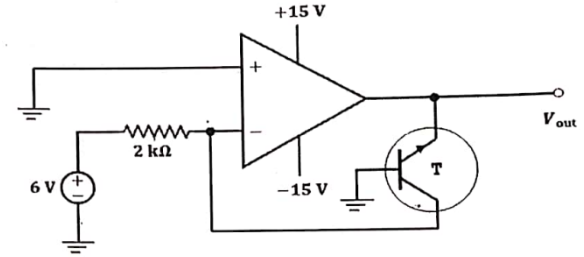
(A)
\(+5.3 \text{V}\)
(B)
\(-0.7 \text{V}\)
(C)
\(+0.7 \text{V}\)
(D)
\(-15 \text{V}\)
Check Answer
Option B
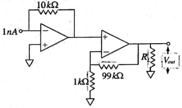
Q.No:8 JEST-2021
What is the output voltage of the following circuit for the input current \(1 nA\)?
(a)
\(1 V\)
(b)
\(1 mV\)
(c)
\(1 \mu V\)
(d)
\(1 nV\)
Check Answer
Option a
Q.No: 9 JEST-2023
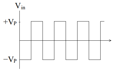
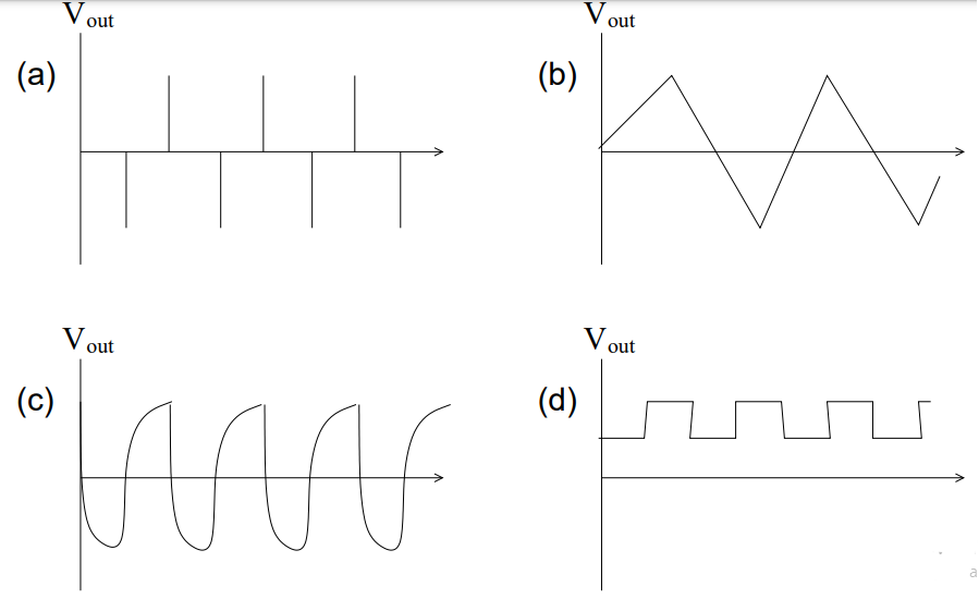
Consider the Op-Amp differentiator presented in Figure (a). Take C = 0.002 \(\mu\)F and \(R_f\) = 2 k\(\Omega\). For a triangular wave input shown in the figure (b),
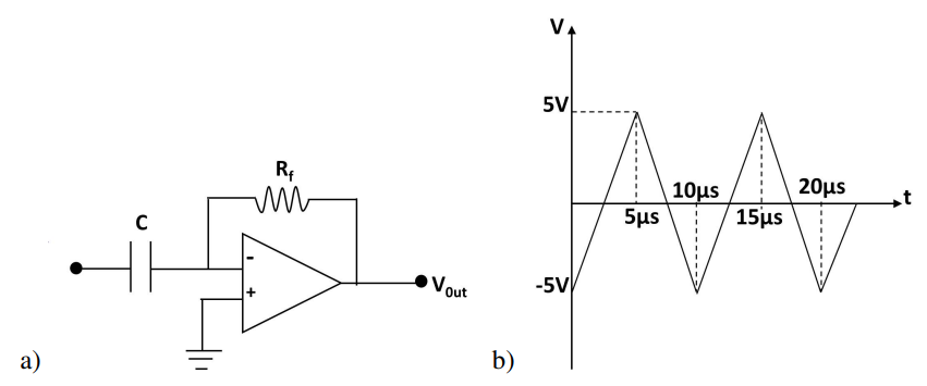
determine the output voltage waveform.


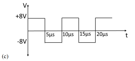
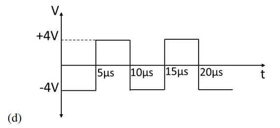
Check Answer
Option a
Q.No: 10 JEST-2024
What is the output voltage \( V_o \) and current \( I \) in the \( 10 \) k\(\Omega\) resistance of the following circuit? \( V_i = 0.5 \) V.
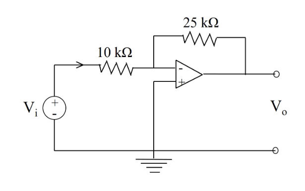
(A) \( V_o = -1.25 \) V, \( I = 50 \) \(\mu\)A
(B) \( V_o = -0.4 \) V, \( I = 50 \) \(\mu\)A
(C) \( V_o = -0.4 \) V, \( I = 20 \) \(\mu\)A
(D) \( V_o = -1.25 \) V, \( I = 20 \) \(\mu\)A
Check Answer
Option A
Q.No:1 TIFR-2012
Consider the following circuit:

If the waveform given below is fed in at
then the waveform at the output \(V_{out}\) will be
Check Answer
Option a
Q.No:2 TIFR-2013
An input of \(1.0 V\) DC is given to the ideal Op-Amp circuit depicted below. What will be the output voltage?

(a)
\(10.0 V\)
(b)
\(-9.0 V\)
(c)
\(1.0 V\)
(d)
\(0 V\)
Check Answer
Option c
Q.No:3 TIFR-2014
In the following circuit, the resistance \(R_2\) is doubled.

It follows that the current through \(R_2\)
(a)
remains the same.
(b)
is halved.
(c)
is doubled.
(d)
is quadrupled.
Check Answer
Option a
Q.No:4 TIFR-2015
In the circuit shown below, the op-amp is powered by a bipolar supply of \(\pm 10 V\).

Which one of the following graphs represents \(V_{\text{out}}\) correctly?

Check Answer
Option d
Q.No:5 TIFR-2016
In the generalized operational amplifier circuit shown on the right, the op. amp. has a very high input impedance (\(Z>50 M \Omega\)) and an open gain of \(1000\) for the frequency range under consideration. Assuming that the op. amp. draws negligible current, the voltage ratio \(V_2/V_1\) is approximately

(a)
\(-190\)
(b)
\(190\)
(c)
\(-90\)
(d)
\(80\)
Check Answer
Option c
Q.No:6 TIFR-2016
For the circuit depicted on the right, the input voltage \(V_i\) is a simple sinusoid as shown below, where the time period is much smaller compared to the time constant of this circuit.


The voltage \(V_0\) across \(C\) is best represented by

Check Answer
Option c
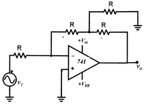
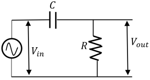
Q.No:7 TIFR-2017
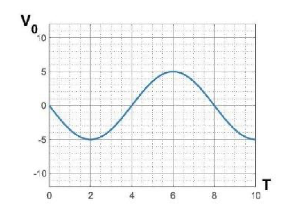
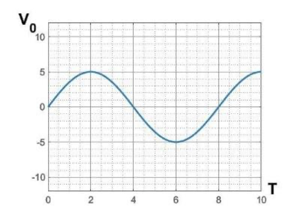
The following circuit is fed with an input sine wave of frequency \(50 \hspace{1mm}\text{Hz}\).

Which of the following graphs (solid line is input and dashed line is output) best represents the correct situation?

Check Answer
Option a
Q.No:8 TIFR-2018
Consider the following circuits C-1 and C-2
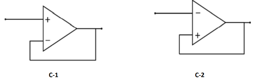
You can apply the golden rules of an ideal op-amp to
(a)
only C-1
(b)
only C-2
(c)
both C-1 and C-2
(d)
neither C-1 nor C-2
Check Answer
Option a
Q.No:9 TIFR-2018
A signal \(V_{\text{in}}(t)=5\sin{(100\pi t)}\) is sent to both the circuits sketched below.

If the DC output voltage of the top circuit has a value \(V_{\text{dc1}}\) and the bottom circuit has a value \(V_{\text{dc2}}\), then which of the following statements about the relative value of \(V_{\text{dc1}}\) and \(V_{\text{dc2}}\) is correct?
(a)
\(V_{\text{dc1}}<V_{\text{dc2}}\)
(b)
\(V_{\text{dc1}}>V_{\text{dc2}}\)
(c)
\(V_{\text{dc1}}=V_{\text{dc2}}\)
(d)
It will depend on the slew rate of the op-amp.
Check Answer
Option b
Q.No:10 TIFR-2018
Consider the circuit shown on the right, which involves an op-amp and two resistors, with an input voltage marked INPUT.

Which of the following circuit components, when connected across the input terminals, is most likely to create a problem in the normal operation of the circuit?
(a)
A voltage source with very high Thevenin resistance.
(b)
A current source with a very high Norton resistance.
(c)
A voltage source with a very low Thevenin resistance.
(d)
A current source with a very low Norton resistance.
Check Answer
Option c
Q.No:11 TIFR-2019
Consider the following circuit.

It is given that \(C_f=100 \hspace{1mm}\text{pF}\), and for \(I_{\text{in}}=50 \hspace{1mm}\text{nA}\) D.C., \(V_{\text{out}}=1\hspace{1mm}\text{V}\) D.C. Therefore, the bandwidth of the above circuit is
(a)
\(15.8 \hspace{1mm}\text{Hz}\)
(b)
\(79.6 \hspace{1mm}\text{Hz}\)
(c)
\(145.3 \hspace{1mm}\text{Hz}\)
(d)
\(200.4 \hspace{1mm}\text{Hz}\)
Check Answer
Option b
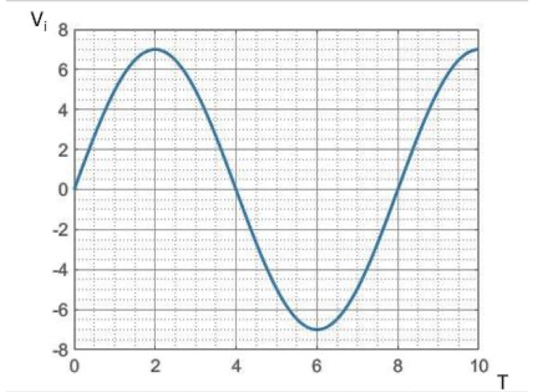
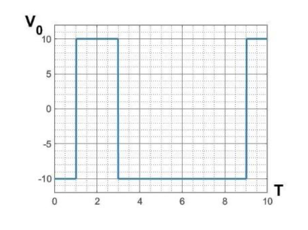
Q.No:12 TIFR-2020
In the below circuit, which of the following is the maximum value, in Volts, of voltage at \(V_{\text{out}}\)?

(a)
\(10\)
(b)
\(15\)
(c)
\(0\)
(d)
\(5\)
Check Answer
Option a
Q.No:13 TIFR-2020
The circuit sketched below is called a relaxation oscillator.

For the parameters indicated in the figure, the ratio of the maximum voltage at \(V_{\text{out}}\) to the maximum voltage at \(V_c\) is
(a)
\(1/8\)
(b)
\(1/7\)
(c)
\(2/7\)
(d)
\(1/4\)
Check Answer
Option a
Q.No:14 TIFR-2021
An operational amplifier is configured as shown in the figure below. For an AC input this circuit behaves effectively as
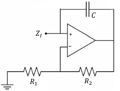
(a)
a capacitor with a negative capacitance.
(b)
an inductor with a negative inductance.
(c)
a resistor with a negative resistance.
(d)
an inductor with a positive inductance
Check Answer
Option a
Q.No:15 TIFR-2021
Consider the following circuit with an op-amp.

If the output voltage \(V_0\) is measured to be \(V_0=-V\), then the value of the feedback resistance \(R_f\) must be
(a)
\(R_f=\frac{6R}{n(n+1)(2n+1)}\)
(b)
\(R_f=\frac{3R}{n(n+1)(2n+1)}\)
(c)
\(R_f=nR\)
(d)
\(R_f=R/n\)
Check Answer
Option a
Q.No:16 TIFR-2021
In an amplifier circuit, an input sine wave of amplitude \(5 \hspace{1mm}\text{V}\) gives a sine wave of amplitude \(25 \hspace{1mm}\text{V}\) as an output in an open load configuration. On applying a \(20 \hspace{1mm}\text{k}\Omega\) load resistance, the output drops to \(10 \hspace{1mm}\text{V}\). This implies that the output resistance of the amplifier must be
(a)
\(30 \hspace{1mm}\text{k}\Omega\)
(b)
\(20 \hspace{1mm}\text{k}\Omega\)
(c)
\(10 \hspace{1mm}\text{k}\Omega\)
(d)
\(2 \hspace{1mm}\text{k}\Omega\)
Check Answer
Option a
Q.No:17 TIFR-2022
Consider a circuit with an operational amplifier (op amp) and four resistors as sketched below.
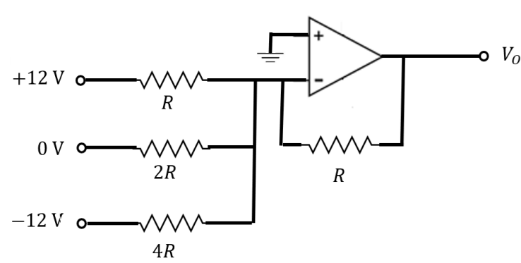
The output voltage \(V_0\) is
(a)
-9 V
(b)
0 V
(c)
-12 V
(d)
-6 V
Check Answer
Option a
Q.No:18 TIFR-2022
It is required to design a circuit with an impedance Z(\(\omega\)) such that
\[Z(\omega)=i k (\omega -\omega_0)\]
for a range of frequencies \(\omega\) such that
\[|\omega-\omega_0|/\omega_0 \ll 1\]
where \(k\) and \(\omega_0\) are constant real numbers.
A possible design for this circuit would correspond to
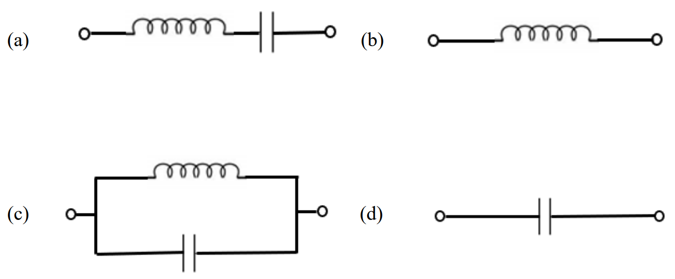
Check Answer
Option a
Q.No:19 TIFR-2022
The non-inverting amplifier shown in the figure on the right is constructed using a nonideal operational amplified (op amp) with a
finite open loop gain \(A\).
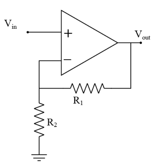
The value of feedback fraction is
\[B=\frac{R_2}{R_1+R_2}=0.1\]
If the gain \(A\) varies such that
\[10^4 < A < 10^5\]
then the approximate percentage variation in
the closed loop gain will be.
(a)
\(0.09\%\)
(b)
\(0.0\%\)
(c)
\(0.9\%\)
(d)
\(9.0\%\)
Check Answer
Option a
Q.No:20 TIFR-2023
At what value of \(R_f\) will the ideal op-amp shown in the figure provide a gain of 6 ?
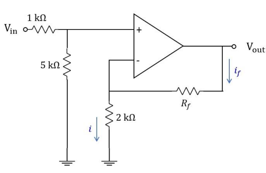
(a)
12.4 \(k \Omega\)
(b)
19.5 \(k \Omega\)
(c)
22.5 \(k \Omega\)
(d)
14.4 \(k \Omega\)
Check Answer
Option a
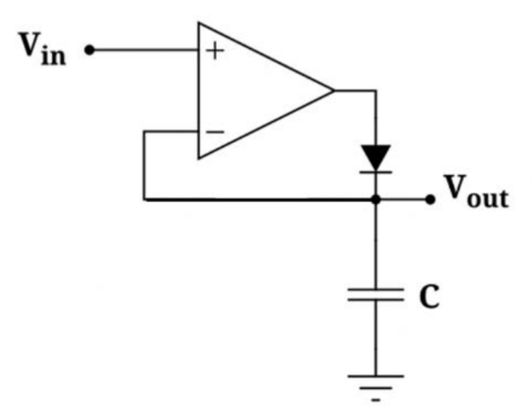
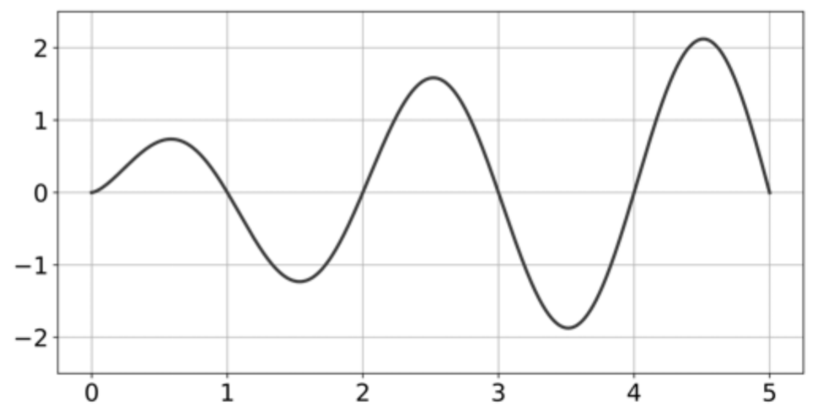
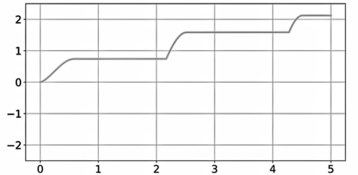
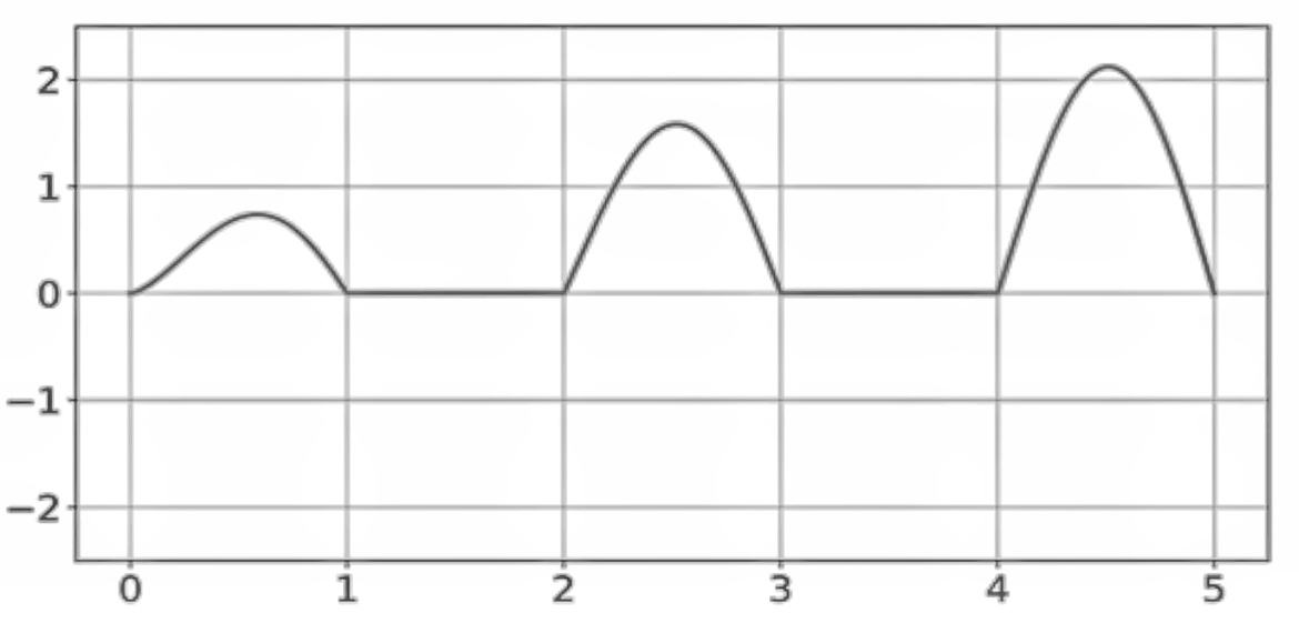
Q.No:21 TIFR-2024
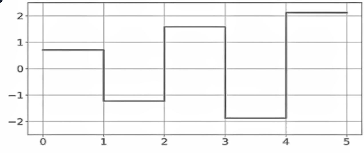
In the following ideal Op-Amp circuit
if the input voltage \( V_i \) is
The output waveform would be

Check Answer
Option 1
Q.No:22 TIFR-2025
The sinusoidal signal
\[
V_{\text{in}} = V_i \sin(2\pi f t)
\]
is given to a high-pass filter (see figure).
The output signal is given by
\[
V_{\text{out}} = V_i |A| \sin(2\pi f t + \phi).
\]
What is the value of \(|A|\)?
a) \(\frac{1}{\sqrt{|1 + \left(\frac{1}{2\pi R C f}\right)^2}|}\)
b) \(\frac{1}{\left|1 + \frac{1}{2\pi R C f}\right|}\)
c) \(\frac{1}{|1 + \left(\frac{1}{2\pi R C f}\right)^2|}\)
d) \(\frac{1}{\sqrt{|1 + \frac{1}{2\pi R C f}|}}\)
Check Answer
Option a
Q.No:23 TIFR-2025
For the circuit shown on the right, which graph represents \(V_{\text{out}}\)
correctly for the \(V_{\text{in}}\) shown below?