
Q.No:1 CSIR June-2015
Consider the circuits shown in Figures (a)

If the transistors in Figures (a) and (b) have current gain \(\beta_{d_c}\) of 100 and 10 respectively. then they operate in the
(1)
active region and saturation region respectively
(2)
saturation region and active region respectively
(3)
saturation region in both cases
(4)
active regio n in both cases
Check Answer
Option 2
Q.No:2 CSIR Dec-2015
Consider an \(n\)-MOSFET with the following parameters: current drive strength \(K=60 \mu\text{A}/\text{V}^2\), breakdown voltage \(BV_{\text{DS}}=10 \text{ V}\), ratio of effective gate width to the channel length \(\frac{W}{L}=5\) and threshold voltage \(V_{th}=0.5 \text{ V}\). In the circuit given below, this \(n\)-MOSFET is operating in the

(1)
ohmic region
(2)
cut-off region
(3)
saturation region
(4)
breakdown region
Check Answer
Option 3
Q.No:3 CSIR June-2017
In the \(n\)-channel JFET shown in figure below, \(V_i=-2V, C=10 pF, V_{DD}=+16 V\), and \(R_D=2 k\Omega\).

If the drain \(D\)-source \(S\) saturation current \(I_{DSS}\) is \(10 mA\) and the pinch-off voltage \(V_P\) is \(-8 V\), then the voltage across points \(D\) and \(S\) is
(1)
\(11.125 V\)
(2)
\(10.375 V\)
(3)
\(5.75 V\)
(4)
\(4.75 V\)
Check Answer
Option 4
Q.No:4 CSIR Dec-2017
In the circuit below the voltages \(V_{BB}\) and \(V_{CC}\) are kept fixed, the voltage measured at B is a constant, but that measured at A fluctuates between a few \(\mu V\) to a few \(mV\).

From these measurements it may be inferred that the
(1)
base is open internally
(2)
emitter is open internally
(3)
collector resistor is open
(4)
base resistor is open
Check Answer
Option 4
Q.No:5 CSIR June-2018
In the following circuit, the value of the common-emitter forward current amplification factor \(\beta\) for the transistor is \(100\) and \(V_{\text{BE}}\) is \(0.7 V\).

The base current \(I_{\text{B}}\) is
(1)
\(40 \mu A\)
(2)
\(30 \mu A\)
(3)
\(44 \mu A\)
(4)
\(33 \mu A\)
Check Answer
Option 4
Q.No:6 CSIR Dec-2018
A sinusoidal signal is an input to the following circuit
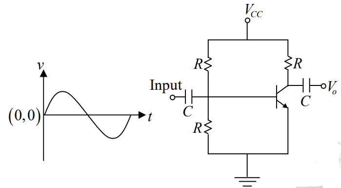
Which of the following graphs best describes the output waveform?


Check Answer
Option 1
Q.No:7 CSIR June-2019
An \(npn\)-transistor is connected in a voltage divider configuration as shown in the figure below.

If the resistor \(R_2\) is disconnected, the voltages \(V_B\) at the base and \(V_C\) at the collector change as follows.
(1)
both \(V_B\) and \(V_C\) increase
(2)
both \(V_B\) and \(V_C\) decrease
(3)
\(V_B\) decreases, but \(V_C\) increases
(4)
\(V_B\) increases, but \(V_C\) decreases
Check Answer
Option 4
Q.No:8 CSIR Sep-2022
The figure below shows a circuit with two transistors, \(Q_1\) and \(Q_2\) having current gain \(\beta_1\) and \(\beta_2\) respectively.

The collector voltage \(V_C\) will be closest to
(1)
\(0.9\) V
(2)
\(2.2\) V
(3)
\(2.9\) V
(4)
\(4.2\) V
Check Answer
Option 2
Q.No:9 CSIR Sep-2022
The circuit containing two n-channel MOSFETs shown below, works as

(1)
a buffer
(2)
a non-inverting amplifier
(3)
an inverter
(4)
a rectifier
Check Answer
Option 3
Q.No:10 CSIR Dec-2024
An LED is required to glow brightly when the temperature sensed by a Platinum
resistance thermometer exceeds a certain value.
In the circuit shown, the resistance of the Pt thermometer (in ohms) varies as
\[
R_{\text{Pt}}(T) = 100 + 0.4T,
\]
where \(T\) is the temperature in degree Celsius.
The transistor turns on when \(V_{BE} > 0.7\ \text{V}\) and it has a very high
current gain.
The temperature at which the LED would start glowing is closest to
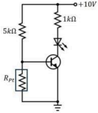
1) 850 °C
2) 400 °C
3) 500 °C
4) 700 °C
Check Answer
Option 4
Q.No:11 CSIR June-2025
The circuit, composed of npn transistors of high \(\beta\), resistors and switches,
is shown in the figure.
The biasing is sufficient to turn on the transistors when the respective switches
\(S_1\) and \(S_2\) are closed.
The voltage across the resistor \(R_x = 100~\text{k}\Omega\) is

1) \(\sim 5~\text{V}\) when both \(S_1\) and \(S_2\) are closed
2) \(\sim 5~\text{V}\) when either \(S_1\) or \(S_2\) are closed
3) \(\sim 5~\text{V}\) when both \(S_1\) and \(S_2\) are open
4) \(\sim 0~\text{V}\) when both \(S_1\) and \(S_2\) are open
Check Answer
Option 3
Q.No:1 GATE-2012
Consider the following circuit in which the current gain \(\beta_{dc}\) of the transistor is \(100\).

Which one of the following correctly represents the load line (collector current \(I_C\) with respect to collector-emitter voltage \(V_{CE}\)) and \(Q\)-point of this circuit?


Check Answer
Option A
Q.No:2 GATE-2013
An \(n\)-channel junction field effect transistor has \(5 mA\) source to drain current at shorted gate (\(I_{\text{DSS}}\)) and \(5 V\) pinch off voltage (\(V_{\text{P}}\)). Calculate the drain current in mA for a gate-source voltage (\(V_{\text{GS}}\)) of \(-2.5 V\). The answer should be up to two decimal places. __________________
Check Answer
Ans 1.25
Q.No:3 GATE-2014
The current gain of the transistor in the following circuit is \(\beta_{dc}=100\). The value of collector current \(I_c\) is ________________ mA.

Check Answer
Ans 1.4-1.7
Q.No:4 GATE-2015
In the given circuit, the voltage across the source resistor is \(1 V\). The drain voltage (in V) is ________.

Check Answer
Ans 15
Q.No:5 GATE-2015
In the simple current source shown in the figure, \(Q_1\) and \(Q_2\) are identical transistors with current gain \(\beta=100\) and \(V_{BE}=0.7 V\)

The current \(I_0\) (in mA) is ________________ (upto two decimal places)
Check Answer
Ans 5.74-5.75
Q.No:6 GATE-2016
For the transistor shown in the figure, assume \(V_{BE}=0.7 V\) and \(\beta_{dc}=100\). If \(V_{in}=5 V\), \(V_{out}\) (in Volts) is ___________. (Give your answer upto one decimal place)

Check Answer
Ans 5.5-5.9
Q.No:7 GATE-2017
For the transistor amplifier circuit shown below with \(R_1=10 k\Omega, R_2=10 k\Omega, R_3=1 k\Omega\), and \(\beta=99\). Neglecting the emitter diode resistance, the input impedance of the amplifier looking into the base for small ac signal is ___________ \(k\Omega\). (up to two decimal places).

Check Answer
Ans 4.75-5.01
Q.No:8 GATE-2018
An n-channel FET having Gate-Source switch-off voltage \(V_{\text{GS(OFF)}}=-2 V\) is used to invert a \(0-5 V\) square-wave signal as shown. The maximum allowed value of \(R\) would be ___________ \(k\Omega\) (up to two decimal places).

Check Answer
Ans 0.70-0.73
Q.No:9 GATE-2024
A typical biasing of a silicon transistor is shown in figure.
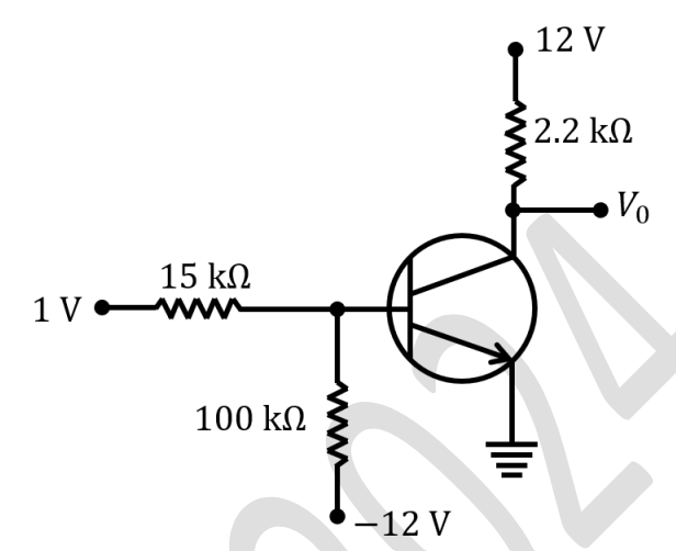
The value of common-emitter current gain \( \beta \) for the transistor is 100. Ignore reverse saturation current. The output voltage \( V_0 \) (in \( V \)) is ___________(in integer).
Check Answer
Ans 12
Q.No:10 GATE-2025
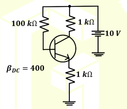
In the transistor circuit shown in the figure,
\(V_{BE} = 0.7~\text{V}\) and \(\beta_{DC} = 400\).
The value of the base current in \(\mu\text{A}\)
(rounded off to one decimal place) is
Check Answer
Ans 18 to 19
Q.No:1 JEST-2016
A transistor in common base configuration has ratio of collector current to emitter current \(\beta\) and ratio of collector to base current \(\alpha\). Which of the following is true?
(A)
\(\beta=\alpha/(\alpha+1)\)
(B)
\(\beta=(\alpha+1)/\alpha\)
(C)
\(\beta=\alpha/(\alpha-1)\)
(D)
\(\beta=(\alpha-1)/\alpha\)
Check Answer
Option A
Q.No:2 JEST-2017
What is the DC base current (approximated to nearest integer value in \(\mu A\)) for the following \(n\)-\(p\)-\(n\) silicon transtisor circuit, given \(R_1=75 \Omega, R_2=4.0 k\Omega, R_3=2.1 k\Omega, R_4=2.6 k\Omega, R_5=6.0 k\Omega, R_6=6.8 k\Omega\), \(C_1=1 \mu F, C_2=2 \mu F\), \(V_{\text{C}}=+15 V\) and \(\beta_{\text{dc}}=75\)?

(A)
\(20\)
(B)
\(24\)
(C)
\(16\)
(D)
\(32\)
Check Answer
Option A
Q.No:3 JEST-2018
Consider the transistor circuit shown in the figure. Assume \(V_{BEQ}=0.7 V, V_{BB}=6 V\)
and the leakage current is negligible. What is the required value of \(R_B\) in kilo-ohms if the base current is to be \(4 \mu A\)?
Check Answer
Ans 1325
Q.No:4 JEST-2020
Analyse the common emitter transistor circuit given in the figure. If the current gain (\(\beta\)) increases by \(50\%\), the relative change in collector current (\(I_C\)) is approximately

(A)
\(5\%\)
(B)
\(15\%\)
(C)
\(20\%\)
(D)
\(25\%\)
Check Answer
Option B
Q.No:5 JEST-2020
Calculate the collector current and determine whether or not the transistor in figure shown below is in saturation. Assume \(V_{CE}(sat)=0.2 V\).

(A)
\(6.5 mA\), not in saturation
(B)
\(11.5 mA\), in saturation
(C)
\(11.5 mA\), not in saturation
(D)
\(6.5 mA\), in saturation
Check Answer
Option A
Q.No:6 JEST-2021
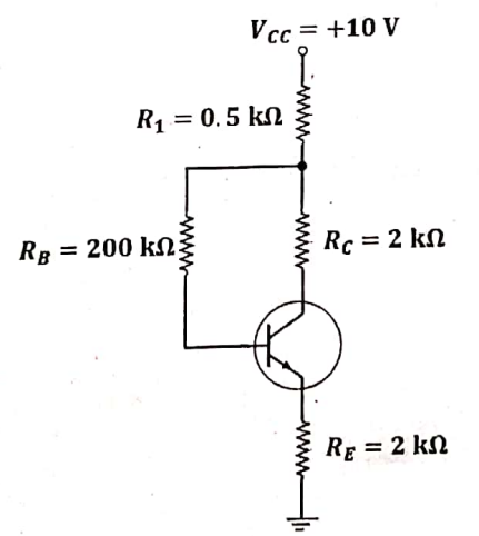
In the following transistor circuit \(R_1=0.5 k\Omega, R_E=R_C=2 k\Omega, R_B=200 k\Omega\),
\(\beta=I_C/I_B=100, V_{CC}=10 \text{V}, V_{BE}=0.7 \text{V}\). Determine the \(V_{CE}\) in \(\text{mV}\)
Check Answer
Ans 950
Q.No:7 JEST-2022
The base current in the first transistor of the following circuit having two identical Silicon-based \(npn\) transistors of \(\beta\) value \(100\), is closest to
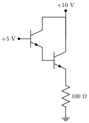
(a)
\(3.6 \mu A\)
(b)
\(0.36 mA\)
(c)
\(5.0 mA\)
(d)
\(5.0 \mu A\)
Check Answer
Option a
Q.No:1 TIFR-2013
The circuit depicted on the right has been made with a silicon n-p-n transistor.

Assuming that there will be a \(0.7 V\) drop across a forward-biased silicon p-n junction, the power dissipated across the transistor will be, approximately,
(a)
\(53 mW\)
(b)
\(94 mW\)
(c)
\(17 mW\)
(d)
\(67 mW\)
Check Answer
Option b
Q.No:2 TIFR-2015
All resistors in the circuit on the right have a tolerance of \(\pm 5\%\).

Assuming a diode drop of \(0.7 V\), which of the following is the lowest possible value of the collector voltage?
(a)
\(3.1 V\)
(b)
\(4.1 V\)
(c)
\(4.7 V\)
(d)
\(5.2 V\)
Check Answer
Option b
Q.No:3 TIFR-2016
In the transistor circuit shown on the right, assume that the voltage drop between the base and the emitter is \(0.5 V\).

What will be the ratio of the resistances \(R_2/R_1\), in order to make this circuit function as a source of constant current, \(I=1 mA\)?
(a)
\(4.5\)
(b)
\(3.0\)
(c)
\(2.5\)
(d)
\(2.0\)
Check Answer
Option d
Q.No:4 TIFR-2017
Which digital logic gate is mimicked by the following silicon diode and silicon transistor circuit?

Check Answer
Ans AND or A.B
Q.No:5 TIFR-2020
The circuit shown below represents a typical voltage-divider bias circuit for a transistor. Assume that resistance values and voltage values are typical for using the transistor as an amplifier.

Which of the following changes in the circuit would result in an increase in the collector voltage \(V_C\)?
(a)
\(R_2\) is decreased slightly
(b)
\(R_2\) is increased slightly
(c)
\(R_c\) is decreased slightly
(d)
\(R_c\) is increased slightly
Check Answer
Option a
Q.No:6 TIFR-2025
Consider the collector–emitter characteristics of a silicon NPN transistor shown
in the figure.
The circuit on the right is used to light an LED with an input voltage
\(V_{\text{in}} = 1\,\text{V}\). The LED needs a current of \(20\,\text{mA}\),
which will be provided by the transistor.
A forward biased silicon PN junction has a \(0.7\,\text{V}\) drop across it.
What is the closest value of the resistor \(R_B\) needed for this purpose?
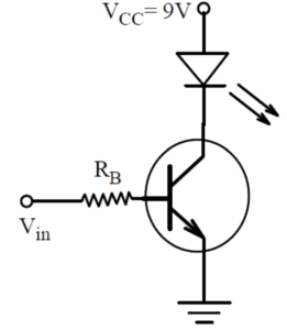

a) \(1.3 k\Omega\)
b) \(560\Omega\)
c) \(4.2 k\Omega\)
d) \(15 k\Omega\)